November 2000
DS92LV1212A
16-40 MHz 10-Bit Bus LVDS Random Lock Deserializer
with Embedded Clock Recovery
General Description
Features
n Clock recovery without SYNC patterns-random lock
n Guaranteed transition every data transfer cycle
The DS92LV1212A is an upgrade of the DS92LV1212. It
maintains all of the features of the DS92LV1212. The
DS92LV1212A is designed to be used with the DS92LV1021
Bus LVDS Serializer. The DS92LV1212A receives a Bus
LVDS serial data stream and transforms it into a 10-bit wide
parallel data bus and separate clock. The reduced cable,
PCB trace count and connector size saves cost and makes
PCB layout easier. Clock-to-data and data-to-data skews are
eliminated since one input receives both clock and data bits
serially. The powerdown pin is used to save power by reduc-
ing the supply current when the device is not in use. The
Deserializer will establish lock to a synchronization pattern
within specified lock times but it can also lock to a data
stream without SYNC patterns.
<
@
n Chipset (Tx + Rx) power consumption 300mW (typ)
40MHz
n Single differential pair eliminates multi-channel skew
n 400 Mbps serial Bus LVDS bandwidth (at 40 MHz clock)
n 10-bit parallel interface for 1 byte data plus 2 control bits
or UTOPIA I Interface
n Synchronization mode and LOCK indicator
n Flow-through pinout for easy PCB layout
n High impedance on receiver inputs when power is off
n Programmable edge trigger on clock
n Footprint compatible with DS92LV1210
n Small 28-lead SSOP package-MSA
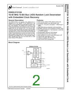
Block Diagram
DS101387-1
TRI-STATE® is a registered trademark of National Semiconductor Corporation.
© 2000 National Semiconductor Corporation
DS101387
www.national.com

 TI [ TEXAS INSTRUMENTS ]