DRV8300-Q1
ZHCSPF5 –APRIL 2022
www.ti.com.cn
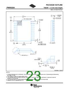
11 Layout
11.1 Layout Guidelines
• Low ESR/ESL capacitors must be connected close to the device between GVDD and GND and between
BSTx and SHx pins to support high peak currents drawn from GVDD and BSTx pins during the turn-on of the
external MOSFETs.
• To prevent large voltage transients at the drain of the top MOSFET, a low ESR electrolytic capacitor and a
good quality ceramic capacitor must be connected between the high side MOSFET drain and ground.
• In order to avoid large negative transients on the switch node (SHx) pin, the parasitic inductances between
the source of the high-side MOSFET and the source of the low-side MOSFET must be minimized.
• In order to avoid unexpected transients, the parasitic inductance of the GHx, SHx, and GLx connections must
be minimized. Minimize the trace length and number of vias wherever possible. Minimum 10 mil and typical
15 mil trace width is recommended.
• Place the gate driver as close to the MOSFETs as possible. Confine the high peak currents that charge and
discharge the MOSFET gates to a minimal physical area by reducing trace length. This confinement
decreases the loop inductance and minimize noise issues on the gate terminals of the MOSFETs.
• Refer to sections General Routing Techniques and MOSFET Placement and Power Stage Routing in
Application Report
Copyright © 2022 Texas Instruments Incorporated
Submit Document Feedback
19
Product Folder Links: DRV8300-Q1

 TI [ TEXAS INSTRUMENTS ]