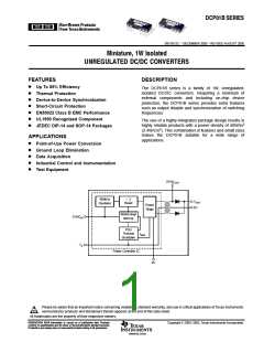
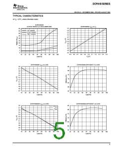
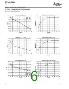
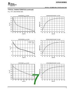
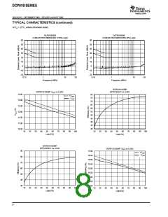
DCP01B SERIES
www.ti.com
SBVS012C − DECEMBER 2000 − REVISED AUGUST 2005
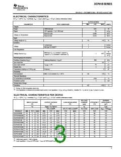
ELECTRICAL CHARACTERISTICS
At T = +25°C, V = nominal, C = 2.2µF, and C
= 0.1µF, unless otherwise noted.
A
S
IN
OUT
DCP01B SERIES
PARAMETER
TEST CONDITIONS
MIN
TYP
MAX
UNITS
Output
Power
Ripple
100% full load
0.97
20
W
O/P capacitor = 1µF, 50% load
Room to cold
mV
PP
0.046
0.016
%/°C
%/°C
Voltage vs Temperature
Room to hot
Input
Voltage range on V
−10
+10
%
S
Isolation
1s flash test
1
1
kVrms
kVrms
Voltage
(1)
60s test, UL1950
Line Regulation
%
change
of V
Minimum V ≤ I constant ≤ typical V
S
S
O
(2)
Voltage Source (V )
S
1
15
Typical V ≤ I constant ≤ maximum V
S
S
O
S
Switching/Synchronization
Oscillator frequency (f
Sync input low
)
Switcing frequency = f /2
OSC
800
kHz
V
OSC
0.4
Sync input current
Disable time
V
= +2V
75
2
µA
µs
pF
SYNC
Capacitance loading on SYNC pin
IN
External
3
Reliability
Demonstrated
MSL 3−(U) versions T = +55°C
−40
−40
+70
°C
A
Thermal Shutdown
IC temperature at shutdown
Shutdown current
Temperature Range
Operating
+150
3
°C
mA
+100
°C
(1)
During UL1950 recognition tests only.
Line regulation is measured at constant load current. Line regulation = (V
(2)
at I
OUT
fixed)/V . Variation % = V min to V typ, V typ to V max.
OUT
S
S
S
S
S
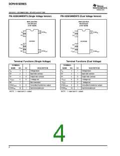
ELECTRICAL CHARACTERISTICS PER DEVICE
At T = +25°C, V = nominal, C = 2.2µF, and C
= 0.1µF, unless otherwise noted.
A
S
IN
OUT
NO LOAD
CURRENT
(mA)
BARRIER
CAPACITANCE
(pF)
INPUT VOLTAGE
(V)
OUTPUT VOLTAGE
(V)
LOAD REGULATION
(%)
EFFICIENCY
(%)
V
S
V
NOM
= V Typical
S
I
Q
C
ISO
(3)
(4)
75% LOAD
10% TO 100% LOAD
0% LOAD
TYP
20
100% LOAD
V
ISO
= 750V
TYP
3.6
RMS
PRODUCT
MIN
4.5
TYP
5
MAX
5.5
MIN
TYP
5
MAX
5.25
TYP
19
18
21
21
19
26
19
11
MAX
31
32
35
38
37
42
41
39
39
23
35
TYP
80
81
81
85
82
82
85
78
80
77
76
DCP010505B
DCP010505DB
DCP010507DB
DCP010512B
DCP010512DB
DCP010515B
DCP010515DB
DCP011512DB
DCP011515DB
DCP012405B
DCP012415DB
4.75
±4.25
±5.75
11.4
4.5
5
5.5
±5
±5.75
±7.25
12.6
22
3.8
4.5
5
5.5
±6.5
12
38
3.0
4.5
5
5.5
29
5.1
4.5
5
5.5
±11.4
14.25
±12
15
±12.6
15.75
±15.75
±12.6
±15.75
5.25
40
4.0
4.5
5
5.5
34
3.8
4.5
5
5.5
±14.25
±11.4
±15
±12
±15
5
42
4.7
13.5
13.5
21.6
21.6
15
15
24
24
16.5
16.5
26.4
26.4
19
2.5
±14.25
4.75
12
13
10
20
2.5
14
2.5
±14.25
±15
±15.75
17
3.8
(3)
100% load current = 1W/V typical.
S
(4)
Load regulation = (V
at 10% load − V
at 100% load)/V
at 75% load.
OUT
OUT
OUT
3

 TI [ TEXAS INSTRUMENTS ]