DAC8571
www.ti.com
SLAS373A–DECEMBER 2002–REVISED JULY 2003
THEORY OF OPERATION (continued)
Output Amplifier
The output buffer is a gain-of-2 noninverting amplifier capable of generating rail-to-rail voltages at its output,
which gives an output range of 0 V to VDD. It is capable of driving a load of 2 kΩ in parallel with 1000 pF to GND.
The source and sink capabilities (fast settling) of the output amplifier can be seen in the typical curves. The slew
rate is 1 V/µs with a full-scale settling time of 10 µs with the output loaded. The feedback and gain setting
resistors of the amplifier are in the order of 50 kΩ. Their absolute value can be off significantly, but they are
matched to within 0.1%.
The inverting input of the output amplifier is brought out to the VSENSE pin, through the feedback resistor. This
allows for better accuracy in critical applications by tying the VSENSE point and the amplifier output together
directly at the load. Other signal conditioning circuitry may also be connected between these points for specific
applications including current sourcing.
I2C Interface
The DAC8571 uses the I2C interface (see I2C-Bus Specification Version 2.1, January 2000, Philips
Semiconductor) to receive and transmit digital data. I2C is a 2-wire serial interface that allows multiple devices on
the same bus to communicate with each other. The serial bus consists of the serial data (SDA) and serial clock
(SCL) lines. Connections to the SDA and SCL lines of the bus are made through open drain IO pins of each
device on the bus. Since the devices that connect to the bus have open drain outputs, the bus should include
pullup structures. When the bus is not active, both SCL and SDA lines are pulled high by these pullup devices.
The DAC8571 supports the I2C serial bus and data transmission protocol, in all three defined modes: standard
(100 Kbps), fast (400 kBps), and high speed (3.4 Mbps).
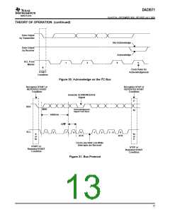
I2C specification states that the device that controls the message is called a master, and the devices that are
controlled by the master are slaves. The master device generates the SCL signal. A master device also
generates special timing conditions (start condition, repeated start condition, and stop condition) on the bus to
indicate the start or stop of a data transfer. Device addressing is also done by the master. The master device on
an I2C bus is usually a microcontroller or a digital signal processor (DSP). The DAC8571 on the other hand,
operates as a slave device on the I2C bus. A slave device acknowledges master's commands and upon master's
control, either receives or transmits data.
I2C specification states that a device that sends data onto the bus is defined as a transmitter, and a device
receiving data from the bus is defined as a receiver. DAC8571 normally operates as a slave receiver. A master
device writes to DAC8571, a slave receiver. However, if a master device inquires DAC8571 internal register data,
DAC8571, operates as a slave transmitter. In this case, the master device reads from the DAC8571, a slave
transmitter. According to I2C terminology, read and write are with respect to the master device.
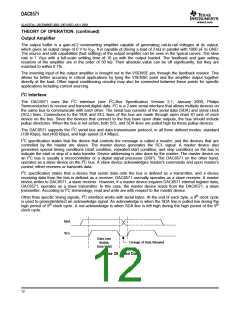
Other than specific timing signals, I2C interface works with serial bytes. At the end of each byte, a 9th clock cycle
is used to generate/detect an acknowledge signal. An acknowledge is when the SDA line is pulled low during the
high period of 9th clock cycle. A not-acknowledge is when SDA line is left high during the high period of the 9th
clock cycle.
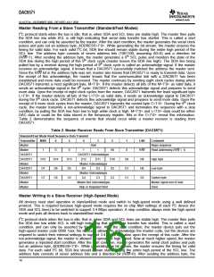
SDA
SCL
Data Line
Change of Data Allowed
Stable;
Data Valid
Figure 29. Valid Data
12

 TI [ TEXAS INSTRUMENTS ]