DAC8571
www.ti.com
SLAS373A–DECEMBER 2002–REVISED JULY 2003
THEORY OF OPERATION
D/A SECTION
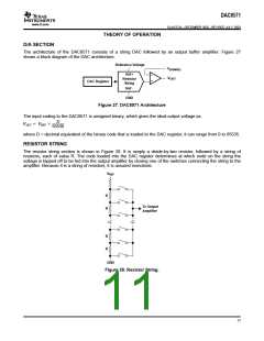
The architecture of the DAC8571 consists of a string DAC followed by an output buffer amplifier. Figure 27
shows a block diagram of the DAC architecture.
Reference Voltage
V
(SENSE)
_
+
Ref+
Resistor
String
V
OUT
DAC Register
Ref-
GND
Figure 27. DAC8571 Architecture
The input coding to the DAC8571 is unsigned binary, which gives the ideal output voltage as:
D
65536
VOUT + VREF
where D = decimal equivalent of the binary code that is loaded to the DAC register; it can range from 0 to 65535.
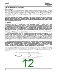
RESISTOR STRING
The resistor string section is shown in Figure 28. It is simply a divide-by-two resistor, followed by a string of
resistors, each of value R. The code loaded into the DAC register determines at which node on the string the
voltage is tapped off to be fed into the output amplifier by closing one of the switches connecting the string to the
amplifier. Because it is a string of resistors, it is assured monotonic.
V
REF
R
To Output
Amplifier
R
R
R
GND
Figure 28. Resistor String.
11

 TI [ TEXAS INSTRUMENTS ]