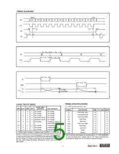
TIMING DIAGRAMS
(MSB)
(LSB)
D0
SDI
CLK
CS
D11
D10
D9
D8
D7
D6
D5
D4
D3
D2
D1
tCSS
tCSH
tLD1
tLD2
LD
tDS
tDH
SDI
tCL
tCH
CLK
tLDW
LD
tCLRW
CLR
FS
tS
tS
±1 LSB
Error Band
VOUT
ZS
TIMING SPECIFICATIONS
LOGIC TRUTH TABLE
TA = –40°C to +85°C and VDD = +5V.
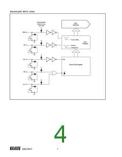
SERIAL SHIFT
REGISTER
CS(1) CLK(1) CLR
LD
DAC REGISTER
SYMBOL
tCH
DESCRIPTION
MIN TYP MAX UNITS
H
L
X
L
H
H
H
H
H
H
H
H
H
H
H
↓
No Change
No Change
No Change
No Change
No Change
No Change
Clock Width HIGH
Clock Width LOW
Load Pulse Width
Data Setup
30
30
20
15
15
30
15
10
30
20
ns
ns
ns
ns
ns
ns
ns
ns
ns
ns
No Change
tCL
L
H
↑
No Change
tLDW
tDS
L
Advanced One Bit
Advanced One Bit
No Change
↑
H(2)
L
tDH
Data Hold
X
Changes to Value of
Serial Shift Register
tCLRW
tLD1
Clear Pulse Width
Load Setup
H(2)
H
X
X
X
H
L
↑
L(3) No Change
Transparent
X
H
No Change
No Change
Loaded with 000H
Latched with 000H
tLD2
Load Hold
H
tCSS
tCSH
Select
↑ Positive Logic Transition; ↓ Negative Logic Transition; X = Don’t Care.
Deselect
NOTES: (1) CS and CLK are interchangeable. (2) A HIGH value is suggested
in order to avoid to “false clock” from advancing the shift register and changing
the DAC voltage. (3) If data is clocked into the serial register while LD is LOW,
the DAC output voltage will change, reflecting the current value of the serial
shift register.
NOTE: All input control signals are specified with tR = tF = 5ns (10% to 90%
of +5V) and timed from a voltage level of 1.6V. These parameters are
guaranteed by design and are not subject to production testing.
®
5
DAC7611

 TI [ TEXAS INSTRUMENTS ]