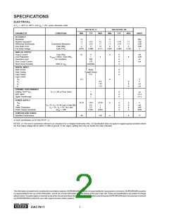
PIN CONFIGURATION
PIN DESCRIPTION
Top View
DIP
PIN
1
LABEL
VDD
DESCRIPTION
Power Supply
2
CS
Chip Select (active LOW).
Synchronous Clock for the Serial Data Input.
1
8
7
6
5
VOUT
GND
CLR
LD
VDD
3
CLK
SDI
2
CS
4
Serial Data Input. Data is clocked into the internal
serial register on the rising edge of CLK.
DAC7611
3
CLK
5
6
LD
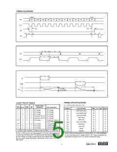
Loads the Internal DAC Register. NOTE: The DAC
register is a transparent latch and is transparent
when LD is LOW (regardless of the state of CS or
CLK).
4
SDI
CLR
Asynchronous Input to Clear the DAC Register.
When CLR is strobbed LOW, the DAC register is set
to 000H and the output voltage to 0V.
PIN CONFIGURATION
7
8
GND
VOUT
Ground
Top View
SOIC
Voltage Output. Fixed output voltage range of ap-
proximately 0V to 4.095V (1mV/LSB). The internal
reference maintains this output range over time,
temperature, and power supply variations (within
the values defined in the specifications section).
1
8
7
6
5
VOUT
GND
CLR
LD
VDD
2
CS
DAC7611
3
CLK
4
SDI
ELECTROSTATIC
DISCHARGE SENSITIVITY
ABSOLUTE MAXIMUM RATINGS(1)
This integrated circuit can be damaged by ESD. Burr-Brown
recommends that all integrated circuits be handled with
appropriate precautions. Failure to observe proper handling
and installation procedures can cause damage.
VDD to GND .......................................................................... –0.3V to 6V
Digital Inputs to GND ............................................. –0.3V to VDD + 0.3V
VOUT to GND........................................................... –0.3V to VDD + 0.3V
Power Dissipation ........................................................................ 325mW
Thermal Resistance, θJA ............................................................ 150°C/W
Maximum Junction Temperature ................................................. +150°C
Operating Temperature Range ...................................... –40°C to +85°C
Storage Temperature Range ........................................ –65°C to +150°C
Lead Temperature (soldering, 10s) ............................................. +300°C
ESD damage can range from subtle performance degrada-
tion to complete device failure. Precision integrated circuits
may be more susceptible to damage because very small
parametric changes could cause the device not to meet its
published specifications.
NOTE: (1) Stresses above those listed under “Absolute Maximum Ratings”
may cause permanent damage to the device. Exposure to absolute maximum
conditions for extended periods may affect device reliability.
PACKAGE/ORDERING INFORMATION
MINIMUM
RELATIVE
ACCURACY
(LSB)
DIFFERENTIAL
NONLINEARITY
(LSB)
SPECIFICATION
TEMPERATURE
RANGE
PACKAGE
DRAWING
NUMBER(1)
ORDERING
NUMBER(2)
TRANSPORT
MEDIA
PRODUCT
PACKAGE
DAC7611P
DAC7611U
"
DAC7611PB
DAC7611UB
"
±2
±2
"
±1
±1
"
±1
±1
"
±1
±1
"
–40°C to +85°C
–40°C to +85°C
"
–40°C to +85°C
–40°C to +85°C
"
8-Pin DIP
8-Lead SOIC
"
8-Pin DIP
8-Lead SOIC
"
006
182
"
006
182
"
DAC7611P
DAC7611U
DAC7611U/2K5
DAC7611PB
DAC7611UB
DAC7611UB/2K5
Rails
Rails
Tape and Reel
Rails
Rails
Tape and Reel
NOTES: (1) For detailed drawing and dimension table, please see end of data sheet, or Appendix C of Burr-Brown IC Data Book. (2) Models with a slash (/) are
available only in Tape and Reel in the quantities indicated (e.g., /2K5 indicates 2500 devices per reel). Ordering 2500 pieces of “DAC7611/2K5” will get a single
2500-piece Tape and Reel. For detailed Tape and Reel mechanical information, refer to Appendix B of Burr-Brown IC Data Book.
®
3
DAC7611

 TI [ TEXAS INSTRUMENTS ]