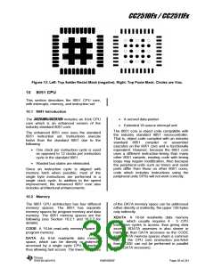
CC2510Fx / CC2511Fx
SFR. A 7-bit read/write register memory
space, which can be directly accessed by a
single CPU instruction. For SFRs whose
address is divisible by eight, each bit is also
individually addressable.
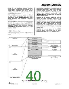
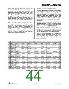
Both the DATA and the SFR memory space is
mapped to the XDATA and CODE memory
space as shown in Figure 14, Figure 15, and
Figure 16 (the CODE and XDATA memory
spaces are mapped identically), and
CC2510FX/CC2511FX has what can be called a
unified memory space.
The four different memory spaces are distinct
in the 8051 architecture, but are partly
overlapping in the CC2510Fx/CC2511Fx to ease
DMA transfers and hardware debugger
operation.
Mapping all the memory spaces to XDATA
allows the DMA controller access to all
physical memory and thus allows DMA
transfers between the different 8051 memory
spaces. This also means that any instruction
that read, write, or manipulate an XDATA
variable can be used on the entire unified
memory space, except writing to or changing
data in flash.
How the different memory spaces are mapped
onto the three physical memories (8/16/32 KB
flash program memory, 1/2/4 KB SRAM, and
hardware registers (SFR, radio, I2S, and USB
(CC2511Fx)) is described in Section 10.2.1 and
Section 10.2.2.
Mapping all memory spaces to the CODE
memory space is primarily done to allow
program execution out of the SRAM/XDATA.
10.2.1 Memory Map
This section gives an overview of the memory
map.
0xFF
0x00
0xFFFF
DATA
Memory Space
Fast Access RAM
0xFF00
0xFEFF
Unimplemented
0xF300
0xF2FF
1 KB SRAM
Slow Access RAM /
0xF000
0xEFFF
Program Memory in RAM
Unimplemented
0xE000
0xDFFF
0xFF
0x80
SFR Memory Space
Hardware SFR Registers
0xDF80
0xDF00
0xDEFF
Hardware Registers
Unimplemented
Hardware Radio Registers /
I2S Registers
0xFFFF
0xDE40
0xDE3F
USB Registers
USB Register (
)
(
)
0xDE00
0xDDFF
Unimplemented
XDATA
Memory Space
0x2000
0x1FFF
0x0000
Non-Volatile Program Memory
8 KB Flash
CC2510F8/CC2511F8 Unified
Memory Space
Physical Memory
0x0000
0xFFFF
CODE
Memory Space
0x0000
8051 Memory Spaces
Figure 14: CC2510F8/CC2511F8 Memory Mapping
SWRS055F
Page 40 of 241

 TI [ TEXAS INSTRUMENTS ]