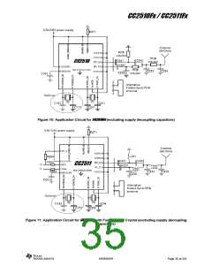
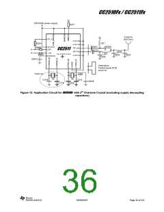
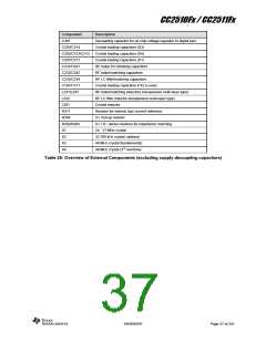
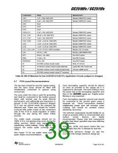
CC2510Fx / CC2511Fx
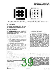
Figure 13: Left: Top Solder Resist Mask (negative). Right: Top Paste Mask. Circles are Vias.
10 8051 CPU
This section describes the 8051 CPU core,
with interrupts, memory, and instruction set.
10.1 8051 Introduction
The CC2510Fx/CC2511Fx includes an 8-bit CPU
core which is an enhanced version of the
industry standard 8051 core.
• A second data pointer
• Extended 18-source interrupt unit
The 8051 core is object code compatible with
the industry standard 8051 microcontroller.
That is, object code compiled with an industry
standard 8051 compiler or assembler
executes on the 8051 core and is functionally
equivalent. However, because the 8051 core
uses a different instruction-timing than many
other 8051 variants, existing code with timing
loops may require modification. Also because
the peripheral units such as timers and serial
ports differ from those on other 8051 cores,
code which includes instructions using the
peripheral units SFRs will not work correctly.
The enhanced 8051 core uses the standard
8051 instruction set. Instructions execute
faster than the standard 8051 due to the
following:
• One clock per instruction cycle is used
as opposed to 12 clocks per instruction
cycle in the standard 8051.
• Wasted bus states are eliminated.
Since an instruction cycle is aligned with
memory fetch when possible, most of the
single byte instructions are performed in a
single clock cycle. In addition to the speed
improvement, the enhanced 8051 core also
includes architectural enhancements:
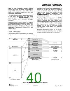
10.2 Memory
The 8051 CPU architecture has four different
memory spaces. The 8051 has separate
memory spaces for program memory and data
memory. The 8051 memory spaces are the
following (see Section 10.2.1 and 10.2.2 for
details):
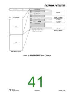
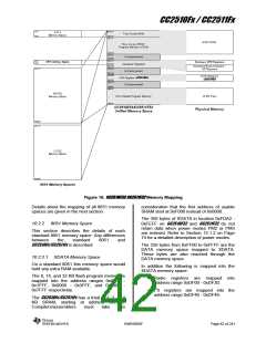
of the DATA memory space can be addressed
either directly or indirectly, the upper 128 bytes
only indirectly.
XDATA. A 16-bit read/write data memory
space, which usually requires 4 - 5 CPU
instruction cycles to access, thus giving slow
access. XDATA assesses is also slower in
hardware than DATA accesses as the CODE
and XDATA memory spaces share a common
bus on the CPU core (instruction pre-fetch
from CODE can not be performed in parallel
with XDATA accesses).
CODE. A 16-bit read-only memory space for
program memory.
DATA. An 8-bit read/write data memory
space, which can be directly or indirectly,
accessed by a single cycle CPU instruction,
thus allowing fast access. The lower 128 bytes
SWRS055F
Page 39 of 241

 TI [ TEXAS INSTRUMENTS ]