CC1110Fx / CC1111Fx
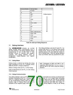
P2_2
P2_1
command
first data byte
second data byte
host input byte
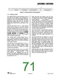
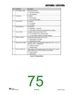
Figure 17: Debug Interface Timing Diagram
11.3 Debug Lock Bit
For software and/or access protection, a set of
lock bits can be written. This information is
contained in the Flash Information Page (see
Section 10.2.3.2), at location 0x000. The Flash
Information Page can only be accessed
through the debug interface. There are three
kinds of lock protect bits as described in this
section.
Note that after the Debug Lock bit has
changed due to a Flash Information Page write
or a flash mass erase, a HALT, RESUME,
DEBUG_INSTR,
STEP_INSTR,
or
STEP_REPLACE command must be executed
so that the Debug Lock value returned by
READ_STATUS shows the updated Debug
Lock value. For example a dummy NOP
DEBUG_INSTR command could be executed.
The Debug Lock bit will also be updated after
a device reset so an alternative is to reset the
chip and reenter debug mode.
The lock size bits LSIZE[2:0] are used to
define which section of the flash memory
should be write protected, if any. The size of
the write protected area can be set to 0 (no
pages), 1, 2, 4, 8, 16, 24, or 32 KB (all pages),
starting from top of flash memory and defining
a section below this. Note that for CC1110F8,
CC1111F8, CC1110F16, and CC1111F16, the only
supported value for LSIZE[2:0]is 0 and 7
(all or no pages respectively).
The CHIP_ERASE command will set all bits in
flash memory to 1. This means that after
issuing a CHIP_ERASE command the boot
sector will be writable, no pages will be write-
protected, and all debug commands are
enabled.
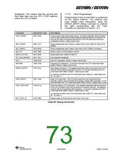
The lock protect bits are written as a normal
flash write to FWDATA(see Section 12.3.2), but
the Debug Interface needs to select the Flash
Information Page first instead of the Flash
Main Page which is the default setting. The
Information Page is selected through the
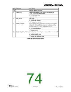
Debug Configuration which is written through
the Debug Interface only. Refer to Section
11.4.1 and Table 46 for details on how the
Flash Information Page is selected using the
Debug Interface.
The second type of lock protect bits is
BBLOCK, which is used to lock the boot sector
page (page 0 ranging from address 0x0000 to
0x03FF). When BBLOCK is set to 0, the boot
sector page is locked.
The third type of lock protect bit is DBGLOCK,
which is used to disable hardware debug
support through the Debug Interface. When
DBGLOCK is set to 0, almost all debug
commands are disabled.
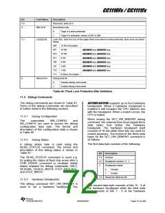
Table 44 defines the byte containing the flash
lock protection bits. Note that this is not an
SFR, but instead the byte stored at location
0x000 in Flash Information Page.
When the Debug Lock bit, DBGLOCK, is set to
0 (see Table 44) all debug commands except
CHIP_ERASE,
READ_STATUS
and
GET_CHIP_ID are disabled and will not
function. The status of the Debug Lock bit can
be read using the READ_STATUS command
(see Section 11.4.2).
SWRS033H
Page 71 of 246

 TI [ TEXAS INSTRUMENTS ]