CC1110Fx / CC1111Fx
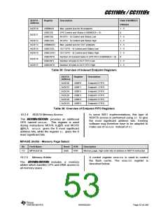
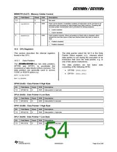
MEMCTR (0xC7) - Memory Arbiter Control
Bit
Field Name
Reset
R/W
Description
7:2
0
R/W
Not used
1
0
R/W
Flash cache disable. Invalidates contents of instruction cache and forces all
instruction read accesses to read straight from flash memory. Disabling will
increase power consumption and is provided for debug purposes.
CACHDIS
0
1
Cache enabled
Cache disabled
0
1
R/W
Flash prefetch disable. When set prefetch of flash data is disabled, when
cleared the next two bytes in flash are fetched when last byte in cache is
read.
PREFDIS
0
1
Prefetch enabled
Prefetch disabled
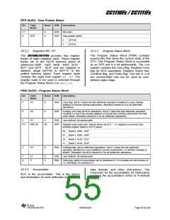
10.3 CPU Registers
This section describes the internal registers
found in the CPU.
The data pointer select bit, bit 0 in the Data
Pointer Select register DPS, chooses which
data pointer to use during the execution of an
instruction that uses the data pointer, e.g. in
one of the above instructions.
10.3.1
Data Pointers
The CC1110Fx/CC1111Fx has two data pointers,
DPTR0 and DPTR1, to accelerate the
movement of data blocks to/from memory. The
data pointers are generally used to access
CODE or XDATA space e.g.
The data pointers are two bytes wide
consisting of the following SFRs:
DPTR0 - DPH0:DPL0
DPTR1 - DPH1:DPL1
MOVC A,@A+DPTR
MOV A,@DPTR.
DPH0 (0x83) - Data Pointer 0 High Byte
Bit
Field Name
Reset
R/W
Description
7:0
DPH0[7:0]
0
R/W
Data pointer 0, high byte
DPL0 (0x82) - Data Pointer 0 Low Byte
Bit
Field Name
Reset
R/W
Description
7:0
DPL0[7:0]
0
R/W
Data pointer 0, low byte
DPH1 (0x85) - Data Pointer 1 High Byte
Bit
Field Name
Reset
R/W
Description
7:0
DPH1[7:0]
0
R/W
Data pointer 1, high byte
DPL1 (0x84) - Data Pointer 1 Low Byte
Bit
Field Name
Reset
R/W
Description
7:0
DPL1[7:0]
0
R/W
Data pointer 1, low byte
SWRS033H
Page 54 of 246

 TI [ TEXAS INSTRUMENTS ]