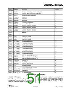
CC1110Fx / CC1111Fx
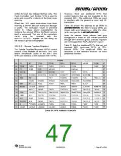
XDATA
Register
Description
Retention7
Address
0xDF14
0xDF15
0xDF16
0xDF17
0xDF18
0xDF19
0xDF1A
0xDF1B
0xDF1C
0xDF1D
0xDF1E
0xDF1F
MCSM0
Main Radio Control State Machine configuration
Frequency Offset Compensation configuration
Bit Synchronization configuration
AGC control
Y
Y
Y
Y
Y
Y
Y
Y
N
N
N
Y
Y
FOCCFG
BSCFG
AGCCTRL2
AGCCTRL1
AGCCTRL0
FREND1
FREND0
FSCAL3
AGC control
AGC control
Front end RX configuration
Front end TX configuration
Frequency synthesizer calibration
Frequency synthesizer calibration
Frequency synthesizer calibration
Frequency synthesizer calibration
Reserved
FSCAL2
FSCAL1
FSCAL0
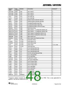
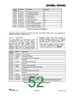
0xDF20
-
0xDF22
0xDF23
0xDF24
0xDF25
0xDF27
0xDF28
0xDF29
0xDF2A
0xDF2B
0xDF2C
0xDF2D
0xDF2E
0xDF2F
0xDF30
0xDF31
0xDF36
0xDF37
0xDF38
0xDF39
0xDF3A
0xDF3B
0xDF3C
0xDF3D
TEST2
Various Test Settings
Y
TEST1
Various Test Settings
Y
TEST0
Various Test Settings
Y
PA_TABLE7
PA_TABLE6
PA_TABLE5
PA_TABLE4
PA_TABLE3
PA_TABLE2
PA_TABLE1
PA_TABLE0
IOCFG2
PA output power setting 7
PA output power setting 6
PA output power setting 5
PA output power setting 4
PA output power setting 3
PA output power setting 2
PA output power setting 1
PA output power setting 0
Radio test signal configuration (P1_7)
Radio test signal configuration (P1_6)
Radio test signal configuration (P1_5)
Chip ID[15:8]
Y
Y
Y
Y
Y
Y
Y
Y
Y
IOCFG1
Y
IOCFG0
Y
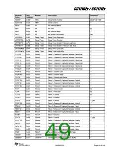
PARTNUM
VERSION
FREQEST
LQI
NA
NA
NA
NA
NA
NA
NA
NA
Chip ID[7:0]
Frequency Offset Estimate
Link Quality Indicator
RSSI
Received Signal Strength Indication
Main Radio Control State
Packet status
MARCSTATE
PKTSTATUS
VCO_VC_DAC PLL calibration current
Table 32: Overview of RF Registers
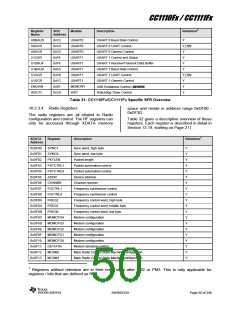
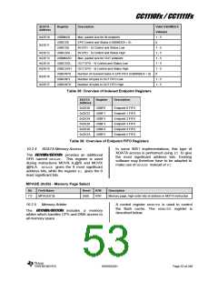
10.2.3.5 I2S Registers
The I2S registers are all related to I2S
configuration and control. The I2S registers can
only be accessed through XDATA memory
space and reside in address range 0xDF40 -
0xDF48. Table 33 gives a descriptive overview
of these registers. Each register is described in
detail in Section 12.15.13, starting on Page
166.
SWRS033H
Page 51 of 246

 TI [ TEXAS INSTRUMENTS ]