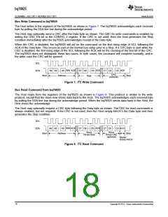
bq76925
SLUSAM9A –JULY 2011–REVISED JULY 2011
www.ti.com
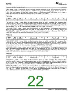
VREF_GAIN_CORR : Lower 4 bits of gain correction factor for reference output. The complete gain correction
factor is obtained by concatenating this value with the most significant bit VREF_GC_4, which is stored in the
VREF_CAL_EXT register. The final value is a 5-bit signed 2’s complement number in the range -16 to +15 with a
value of 0.1% per lsb. See description of usage in OPERATIONAL OVERVIEW.
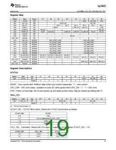
VC1_CAL
Address
Name
Type
D7
D6
D5
D4
D3
D2
D1
D0
0x11
VC1_CAL
EEPROM
VC1_OFFSET_CORR
VC1_GAIN_CORR
VC1_OFFSET_CORR : Lower 4 bits of offset correction factor for cell 1 translation. The complete offset
correction factor is obtained by concatenating this value with the most significant bit VC1_OC_4, which is stored
in the VC_CAL_EXT_1 register. The final value is a 5-bit signed 2’s complement number in the range -16 to +15
with a value of 1 mV per lsb. See description of usage in OPERATIONAL OVERVIEW.
VC1_GAIN_CORR : Lower 4 bits of gain correction factor for cell 1 translation. The complete gain correction
factor is obtained by concatenating this value with the most significant bit VC1_GC_4, which is stored in the
VC_CAL_EXT_1 register. The final value is a 5-bit signed 2’s complement number in the range -16 to +15 with a
value of 0.1% per lsb. See description of usage in OPERATIONAL OVERVIEW.
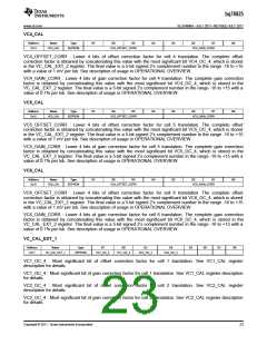
VC2_CAL
Address
Name
Type
D7
D6
D5
D4
D3
D2
D1
D0
0x12
VC2_CAL
EEPROM
VC2_OFFSET_CORR
VC2_GAIN_CORR
VC2_OFFSET_CORR : Lower 4 bits of offset correction factor for cell 2 translation. The complete offset
correction factor is obtained by concatenating this value with the most significant bit VC2_OC_4, which is stored
in the VC_CAL_EXT_1 register. The final value is a 5-bit signed 2’s complement number in the range -16 to +15
with a value of 1 mV per lsb. See description of usage in OPERATIONAL OVERVIEW.
VC2_GAIN_CORR : Lower 4 bits of gain correction factor for cell 2 translation. The complete gain correction
factor is obtained by concatenating this value with the most significant bit VC2_GC_4, which is stored in the
VC_CAL_EXT_1 register. The final value is a 5-bit signed 2’s complement number in the range -16 to +15 with a
value of 0.1% per lsb. See description of usage in OPERATIONAL OVERVIEW.
VC3_CAL
Address
Name
Type
D7
D6
D5
D4
D3
D2
D1
D0
0x13
VC3_CAL
EEPROM
VC3_OFFSET_CORR
VC3_GAIN_CORR
VC3_OFFSET_CORR : Lower 4 bits of offset correction factor for cell 3 translation. The complete offset
correction factor is obtained by concatenating this value with the most significant bit VC3_OC_4, which is stored
in the VC_CAL_EXT_2 register. The final value is a 5-bit signed 2’s complement number in the range -16 to +15
with a value of 1 mV per lsb. See description of usage in OPERATIONAL OVERVIEW.
VC3_GAIN_CORR : Lower 4 bits of gain correction factor for cell 3 translation. The complete gain correction
factor is obtained by concatenating this value with the most significant bit VC3_GC_4, which is stored in the
VC_CAL_EXT_2 register. The final value is a 5-bit signed 2’s complement number in the range -16 to +15 with a
value of 0.1% per lsb. See description of usage in OPERATIONAL OVERVIEW.
22
Copyright © 2011, Texas Instruments Incorporated

 TI [ TEXAS INSTRUMENTS ]