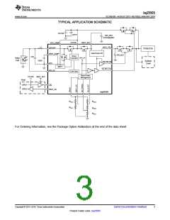
bq25505
www.ti.com
SLUSBJ3B –AUGUST 2013–REVISED JANUARY 2014
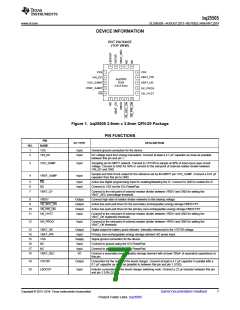
DEVICE INFORMATION
RGT PACKAGE
(TOP VIEW)
20
19
18
17
16
1
2
3
4
5
15
VSS
VIN_DC
VSS
14 VBAT_PRI
bq25505
RGR
3.5x3.5mm
13
VOC_SAMP
VREF_SAMP
EN
VBAT_OK
12
OK_PROG
11
OK_HYST
6
7
8
9
10
Figure 1. bq25505 3.5mm x 3.5mm QFN-20 Package
PIN FUNCTIONS
PIN
NAME
VSS
I/O TYPE
DESCRIPTION
NO.
1
Input
Input
General ground connection for the device
2
VIN_DC
DC voltage input from energy harvesters. Connect at least a 4.7 µF capacitor as close as possible
between this pin and pin 1.
3
VOC_SAMP
VREF_SAMP
Input
Sampling pin for MPPT network. Connect to VSTOR to sample at 80% of input soure open circuit
voltage. Connect to GND for 50% or connect to the mid-point of external resistor divider between
VIN_DC and GND.
Sample and hold circuit output for the reference set by the MPPT per VOC_SAMP. Connect a 0.01 µF
capacitor from this pin to GND.
4
Input
5
6
7
EN
Input
Input
Active low digital programming input for enabling/disabling the IC. Connect to GND to enable the IC.
Connect to VSS via the IC's PowerPad.
NC
VBAT_OV
Connect to the mid-point of external resistor divider between VRDIV and GND for setting the
VBAT_SEC overvoltage threshold.
8
9
VRDIV
Output
Output
Output
Input
Connect high side of resistor divider networks to this biasing voltage.
VB_SEC_ON
VB_PRI_ON
OK_HYST
Active low push-pull driver for the secondary (rechargeable) energy storage PMOS FET.
Active low push-pull driver for the primary (non-rechargeable) energy storage PMOS FET.
10
11
Connect to the mid-point of external resistor divider between VRDIV and GND for setting the
VBAT_OK hysteresis threshold.
12
OK_PROG
Input
Connect to the mid-point of external resistor divider between VRDIV and GND for setting the
VBAT_OK threshold.
13
14
15
16
17
18
VBAT_OK
VBAT_PRI
VSS
Output
Input
Supply
Input
Input
I/O
Digital output for battery good indicator. Internally referenced to the VSTOR voltage.
Primary (non-rechargeable) energy storage element HiZ sense input.
Signal ground connection for the device.
NC
Connect to ground using the IC's PowerPad.
NC
Connect to ground using the IC's PowerPad.
VBAT_SEC
Connect a secondary (rechargeable) storage element with at least 100uF of equivalent capacitance to
this pin.
19
20
VSTOR
Output
Input
Connection for the output of the boost charger. Connect at least a 4.7 µF capacitor in parallel with a
0.1 µF capacitor as close as possible to between this pin and pin 1 (VSS).
LBOOST
Inductor connection for the boost charger switching node. Connect a 22 µH inductor between this pin
and pin 2 (VIN_DC).
Copyright © 2013–2014, Texas Instruments Incorporated
Submit Documentation Feedback
7
Product Folder Links :bq25505

 TI [ TEXAS INSTRUMENTS ]