bq25505
www.ti.com
SLUSBJ3B –AUGUST 2013–REVISED JANUARY 2014
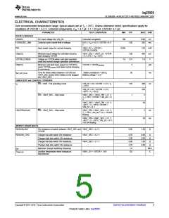
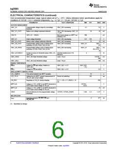
ELECTRICAL CHARACTERISTICS
Over recommended temperature range, typical values are at TA = 25°C. Unless otherwise noted, specifications apply for
conditions of VSTOR = 4.2 V. External components, CIN = 4.7 µF, L1 = 22 µH, CSTOR= 4.7 µF
PARAMETER
TEST CONDITIONS
MIN
TYP
MAX UNIT
BOOST CHARGER
VIN(DC)
DC input voltage into VIN_DC
Cold-start completed
100
5100
285
mV
mA
I-CHG(CBC_LIM)
Cycle-by-cycle current limit of charger
0.5V < VIN < 4.0 V; VSTOR = 4.2
V
230
PIN
Input power range for normal charging
VBAT_OV > VSTOR >
VSTOR_CHGEN
0.005
1.6
510
400
1.9
mW
mV
V
VIN(CS)
Minimum input voltage for cold start circuit to
start charging VSTOR
VBAT_SEC < VBAT_UV; VSTOR
= 0 V; 0°C < TA < 85°C
330
1.73
5
VSTOR_CHGEN
PIN(CS)
Voltage on VSTOR when cold start operation
ends and normal charger operation commences
Minimum cold-start input power for VSTOR to
reach VSTOR(CHGEN) and allow normal charging
to commence
VSTOR < VSTOR(CHGEN)
µW
tBAT_HOT_PLUG
Time for which switch between VSTOR and
VBAT_SEC closes when battery is hot plugged
into VBAT_SEC
Battery resistance = 300 Ω,
Battery voltage = 3.3V
50
325
1
ms
nA
QUIESCENT and LEAKAGE CURRENTS
IQ
EN = GND - Full operating mode
VIN_DC = 0V; VSTOR = 2.1V; TJ
= 25°C
400
700
5
VIN_DC = 0V; VSTOR = 2.1V;
–40°C < TJ < 85°C
EN = VBAT_SEC - Ship mode
EN = VBAT_SEC - Ship mode
VBAT_SEC = VBAT_PRI = 2.1 V;
TJ = 25°C; VSTOR = VIN_DC = 0
V
VBAT_SEC = VBAT_PRI = 2.1 V;
–40°C < TJ < 85°C; VSTOR =
VIN_DC = 0 V
20
5
I-BATPRI(LEAK)
VBAT_PRI = VBAT_SEC = 2.1 V;
TJ = 25°C; VIN_DC = 0 V; VSTOR
floating
1
nA
nA
VBAT_PRI = VBAT_SEC = 2.1 V;
–40°C < TJ < 85°C; VIN_DC = 0 V;
VSTOR floating
20
MOSFET RESISTANCES
RDS(ON)-BAT
ON resistance of switch between VBAT_SEC and VBAT_SEC = 4.2 V
VSTOR
0.95
1.50
Ω
RDS(ON)_CHG
Charger low side switch ON resistance
Charger high side switch ON resistance
Charger low side switch ON resistance
Charger high side switch ON resistance
Maximum charger switching frequency
VBAT_SEC = 4.2 V
0.70
2.30
0.80
3.70
1.0
0.90
3.00
1.00
4.80
Ω
Ω
VBAT_SEC = 2.1 V
Ω
Ω
fSW
MHz
C
TTEMP_SD
Junction temperature when charging is
discontinued
VBAT_OV > VSTOR > 1.8V
125
Copyright © 2013–2014, Texas Instruments Incorporated
Submit Documentation Feedback
5
Product Folder Links :bq25505

 TI [ TEXAS INSTRUMENTS ]