bq24296
bq24297
www.ti.com
SLUSBP6A –SEPTEMBER 2013–REVISED OCTOBER 2013
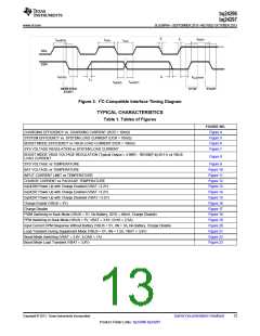
Figure 3. I2C-Compatible Interface Timing Diagram
TYPICAL CHARACTERISTICS
Table 1. Tables of Figures
FIGURE NO.
Figure 4
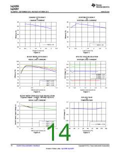
CHARGING EFFICIENCY vs. CHARGING CURRENT (DCR = 10mΩ)
SYSTEM EFFICIENCY vs. SYSTEM LOAD CURRENT (DCR = 10mΩ)
BOOST MODE EFFICIENCY vs VBUS LOAD CURRENT (DCR = 10mΩ)
SYS VOLTAGE REGULATION vs SYSTEM LOAD CURRENT
Figure 5
Figure 6
Figure 7
BOOST MODE VBUS VOLTAGE REGULATION (Typical Output = 4.998V ; REG06[7:4]=0111) vs VBUS
LOAD CURRENT
Figure 8
SYS VOLTAGE vs TEMPERATURE
Figure 9
Figure 10
Figure 11
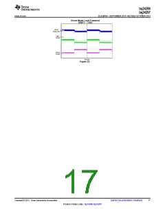
Figure 12
Figure 13
Figure 14
Figure 15
Figure 16
Figure 17
Figure 18
Figure 19
Figure 20
Figure 21
Figure 22
Figure 23
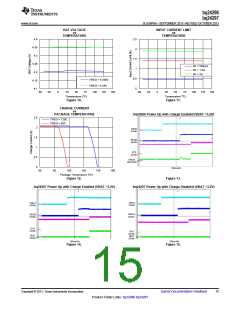
BAT VOLTAGE vs TEMPERATURE
INPUT CURRENT LIMIT vs TEMPERATURE
CHARGE CURRENT vs PACKAGE TEMPERATURE
bq24296 Power Up with Charge Enabled (VBAT =3.2V)
bq24297 Power Up with Charge Enabled (VBAT =3.2V)
bq24297 Power Up with Charge Disabled (VBAT =3.2V)
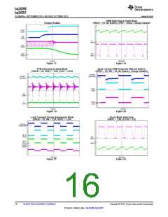
Charge Enable (VBUS = 5V)
Charge Disable
PWM Switching in Buck Mode (VBUS = 5V, No Battery, ISYS = 40mA, Charge Disable)
PFM Switching in Buck Mode (VBUS = 5V, VBAT = 3.6V, ICHG = 2.5A)
Input Current DPM Response Without Battery (VBUS = 5V, IIN = 3A, No Battery, Charge Disable
Load Transient During Supplement Mode (VBUS = 5V, IIN = 1.5A, VBAT = 3.8V)
Boost Mode Switching (VBAT = 3.8V, ILOAD = 1A)
Boost Mode Load Transient (VBAT = 3.8V)
Copyright © 2013, Texas Instruments Incorporated
Submit Documentation Feedback
13
Product Folder Links: bq24296 bq24297

 TI [ TEXAS INSTRUMENTS ]