bq24160, bq24161
bq24163, bq24168
SLUSAO0A –NOVEMBER 2011–REVISED MARCH 2012
www.ti.com
PCB Layout Guidelines
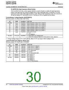
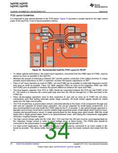
It is important to pay special attention to the PCB layout. Figure 32 provides a sample layout for the high current
paths of the bq2416x. A list of layout guidelines follows.
PMIDU USB
PMIDI
SW
IN
PGND
SYS
PGND
BOOT
BAT
SW
SYS
Figure 32. Recommended bq2416x PCB Layout for WCSP
•
•
•
To obtain optimal performance, the power input capacitors, connected from the PMID input to PGND, must be
placed as close as possible to the bq2416x
Minimize the amount of inductance between BAT and the postive connection of the battery terminal. If a large
parasitic board inductance on BAT is expected, increase the bypass capacitance on BAT.
Place 4.7µF input capacitor as close to PMID_ pin and PGND pin as possible to make high frequency current
loop area as small as possible. Place 1µF input capacitor GNDs as close to the respective PMID cap GND
and PGND pins as possible to minimize the ground difference between the input and PMID_.
•
•
•
The local bypass capacitor from SYS to GND should be connected between the SYS pin and PGND of the
IC. The intent is to minimize the current path loop area from the SW pin through the LC filter and back to the
PGND pin.
Place all decoupling capacitors close to their respective IC pins and as close as to PGND (do not place
components such that routing interrupts power stage currents). All small control signals should be routed
away from the high-current paths.
The PCB should have a ground plane (return) connected directly to the return of all components through vias
(two vias per capacitor for power-stage capacitors, one via per capacitor for small-signal components). It is
also recommended to put vias inside the PGND pads for the IC, if possible. A star ground design approach is
typically used to keep circuit block currents isolated (high-power/low-power small-signal) which reduces noise-
coupling and ground-bounce issues. A single ground plane for this design gives good results. With this small
layout and a single ground plane, there is no ground-bounce issue, and having the components segregated
minimizes coupling between signals.
•
•
The high-current charge paths into IN, USB, BAT, SYS and from the SW pins must be sized appropriately for
the maximum charge current in order to avoid voltage drops in these traces. The PGND pins should be
connected to the ground plane to return current through the internal low-side FET.
For high-current applications, the balls for the power paths should be connected to as much copper in the
board as possible. This allows better thermal performance because the board conducts heat away from the
IC.
34
Submit Documentation Feedback
Copyright © 2011–2012, Texas Instruments Incorporated
Product Folder Link(s): bq24160 bq24161 bq24163 bq24168

 TI [ TEXAS INSTRUMENTS ]