AM6548, AM6528, AM6526
ZHCSLA7B –DECEMBER 2019 –REVISED JUNE 2021
www.ti.com.cn
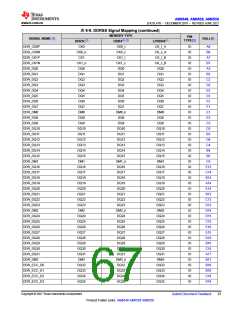
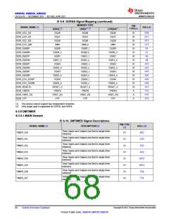
表6-9. DDRSS Signal Mapping (continued)
MEMORY TYPE
DDR4(1) (2)
DQ36
PIN
TYPE[3]
SIGNAL NAME [1]
DDR_ECC_D4
BALL[4]
DDR3L(2)
DQ36
LPDDR4(1)
DQ36
IO
IO
IO
IO
IO
IO
IO
IO
IO
IO
IO
IO
IO
IO
IO
A
E18
E17
D17
C17
D1
DDR_ECC_D5
DDR_ECC_D6
DDR_ECC_DM
DDR_DQS0P
DDR_DQS0N
DDR_DQS1P
DDR_DQS1N
DDR_DQS2P
DDR_DQS2N
DDR_DQS3P
DDR_DQS3N
DDR_ECC_DQSP
DDR_ECC_DQSN
DDR_RESETn
DDR_VREF0
DDR_VREF_ZQ
DDR_VTP
DQ37
DQ37
DQ37
DQ38
DQ38
DQ38
DM4
DM4_n
DM4
DQS0
DQS0_t
DQS0_c
DQS1_t
DQS1_c
DQS2_t
DQS2_c
DQS3_t
DQS3_c
DQS4_t
DQS4_c
RESET_n
VREF0
DQS0
DQS0_n
DQS1
DQS0_n
DQS1
C1
A5
DQS1_n
DQS2
DQS1_n
DQS2
A4
A13
A12
A15
A16
A19
A18
A11
F12
F15
F13
DQS2_n
DQS3
DQS2_n
DQS3
DQS3_n
DQS4
DQS3_n
DQS4
DQS4_n
RESET_n
VREF0
VREF_ZQ
VTP
DQS4_n
RESET_n
VREF0
VREF_ZQ
VTP
VREF_ZQ
VTP
A
A
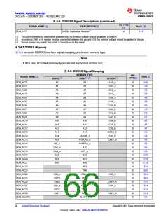
(1) This device cannot support two independent channels.
(2) Only single rank is supported for DDR3L and DDR4.
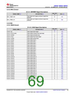
6.3.5 DMTIMER
6.3.5.1 MAIN Domain
表6-10. DMTIMER Signal Descriptions
PIN TYPE
SIGNAL NAME [1]
DESCRIPTION [2]
BALL [4]
B22
[3]
Timer Inputs and Outputs (not tied to single timer
instance)
TIMER_IO0
TIMER_IO1
TIMER_IO2
TIMER_IO3
TIMER_IO4
TIMER_IO5
TIMER_IO6
TIMER_IO7
IO
IO
IO
IO
IO
IO
IO
IO
Timer Inputs and Outputs (not tied to single timer
instance)
C23
Timer Inputs and Outputs (not tied to single timer
instance)
P23
Timer Inputs and Outputs (not tied to single timer
instance)
R23
Timer Inputs and Outputs (not tied to single timer
instance)
AG11
AD11
T24
Timer Inputs and Outputs (not tied to single timer
instance)
Timer Inputs and Outputs (not tied to single timer
instance)
Timer Inputs and Outputs (not tied to single timer
instance)
T23
Copyright © 2021 Texas Instruments Incorporated
68
Submit Document Feedback
Product Folder Links: AM6548 AM6528 AM6526

 TI [ TEXAS INSTRUMENTS ]