AM6548, AM6528, AM6526
ZHCSLA7B –DECEMBER 2019 –REVISED JUNE 2021
www.ti.com.cn
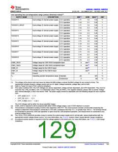
over operating free-air temperature range (unless otherwise noted)(2)
SUPPLY NAME
DESCRIPTION
Dual-voltage IO domain power supply 1.8-V operation
3.3-V operation
MIN(1)
1.71
3.14
1.71
3.14
1.71
3.14
1.71
3.14
1.71
3.14
1.71
3.14
1.71
3.14
1.71
3.14
0
NOM
1.8
MAX(1)
1.89
3.46
1.89
3.46
1.89
3.46
1.89
3.46
1.89
3.46
1.89
3.46
1.89
3.46
1.89
3.46
1.89
1.89
UNIT
V
VDDSHV2
3.3
V
VDDSHV2_WKUP
VDDSHV3
Dual-voltage IO domain power supply 1.8-V operation
3.3-V operation
1.8
V
3.3
V
Dual-voltage IO domain power supply 1.8-V operation
3.3-V operation
1.8
V
3.3
V
VDDSHV4
Dual-voltage IO domain power supply 1.8-V operation
3.3-V operation
1.8
V
3.3
V
VDDSHV5
Dual-voltage IO domain power supply 1.8-V operation
3.3-V operation
1.8
V
3.3
V
VDDSHV6
Dual-voltage IO domain power supply 1.8-V operation
3.3-V operation
1.8
V
3.3
V
VDDSHV7
Dual-voltage IO domain power supply 1.8-V operation
3.3-V operation
1.8
V
3.3
V
VDDSHV8
Dual-voltage IO domain power supply 1.8-V operation
3.3-V operation
1.8
V
3.3
V
USB0_VBUS
USB1_VBUS
USB0_ID
USB1_ID
VSS
Voltage range for USB VBUS comparator input
Voltage range for USB VBUS comparator input
Voltage range for the USB ID input
Voltage range for the USB ID input
Ground
see(7)
see(7)
see(5)
see(5)
0
V
0
V
V
V
V
TJ
Operating junction temperature range Extended
Commercial
-40
0
105
90
°C
°C
(1) The voltage at the device ball must never be below the MIN voltage or above the MAX voltage for any amount of time. This
requirement includes dynamic voltage events such as AC ripple, voltage transients, voltage dips, and so forth.
(2) Refer to Power-On-Hour (POH) Limits for limitations.
(3) This value is without AVS. The AVS Voltages are device-dependent, voltage domain-dependent, and OPP-dependent. They must be
read from the VTM_DEVINFO_VDn. For information about VTM_DEVINFO_VDn registers address, please refer to section Voltage
and Thermal Manager (VTM) in the device TRM. The power supply should be adjustable over the following ranges for each required
OPP:
•
•
•
OPP_NOM: 0.9 V –1.1 V
OPP_OD: 0.9 V –1.2 V
OPP_TURBO: 0.9 V –1.24 V
The AVS Voltages will be within the above specified ranges.
(4) VDDS_DDR is required to still be powered with either DDR4 voltage ranges, even If DDR interface is unused.
(5) This terminal is connected to analog circuits in the respective USB PHY. The circuit sources a known current while measuring the
voltage to determine if the terminal is connected to VSS with a resistance less than 10 Ωor greater than 100 kΩ. The terminal should
be connected to ground for USB host operation or open-circuit for USB peripheral operation, and should never be connected to any
external voltage source.
(6) The VDDA_VSYS_MON pin provides a way to monitor the system power supply and is not fail-safe, unless implemented with the
appropriate resistor voltage divider source. For more information, see 节9.2.5, System Power Supply Monitor Design Guidelines.
(7) An external resistor divider is required to limit the voltage applied to this device pin. For more information, see 节9.2.3, USB Design
Guidelines.
Copyright © 2021 Texas Instruments Incorporated
Submit Document Feedback 129
Product Folder Links: AM6548 AM6528 AM6526

 TI [ TEXAS INSTRUMENTS ]