AM6548, AM6528, AM6526
ZHCSLA7B –DECEMBER 2019 –REVISED JUNE 2021
www.ti.com.cn
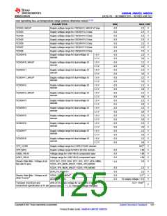
over operating free-air temperature range (unless otherwise noted)(1) (2)
PARAMETERS
MIN
MAX UNIT
(6)
TSTG
Storage temperature
-55
+150 °C
(1) Stresses beyond those listed under Absolute Maximum Ratings may cause permanent damage to the device. These are stress ratings
only, and functional operation of the device at these or any other conditions beyond those indicated under 节7.4, Recommended
Operating Conditions is not implied. Exposure to absolute-maximum-rated conditions for extended periods may affect device reliability.
(2) All voltage values are with respect to their associated VSS or VSSA_x, unless otherwise noted.
(3) This parameter applies to all IO pins which are not fail-safe and the requirement applies to all values of IO supply voltage. For
example, if the voltage applied to a specific IO supply is 0 volts the valid input voltage range for any IO powered by that supply will be
–0.3 to +0.3 volts. Special attention should be applied anytime peripheral devices are not powered from the same power sources
used to power the respective IO supply. It is important the attached peripheral never sources a voltage outside the valid input voltage
range, including power supply ramp-up and ramp-down sequences.
(4) The VDDA_VSYS_MON pin provides a way to monitor the system power supply and is not fail-safe, unless implemented with the
appropriate resistor voltage divider source. For more information, see 节9.2.5, System Power Supply Monitor Design Guidelines.
(5) VDD is the voltage on the corresponding power-supply pin(s) for the IO.
(6) For tape and reel the storage temperature range is [–10°C; +50°C] with a maximum relative humidity of 70%. TI recommends
returning to ambient room temperature before usage.
(7) The voltage on the VDDA_VSYS_MON pin should never exceed VDDA_POR_WKUP’s voltage.
(8) NC stands for No Connect.
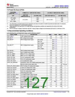
Fail-safe IO terminals are designed such they do not have dependencies on the respective IO power supply
voltage. This allows external voltage sources to be connected to these IO terminals when the respective IO
power supplies are turned off. The I2C0_SCL, I2C0_SDA, I2C1_SCL, I2C1_SDA, DDR_FS_RESETn, NMIn,
VDDA_1P8_MON_WKUP, VDDA_1P8_MON0, VDDA_3P3_MON_WKUP, and VDDA_3P3_MON0 are the only
fail-safe IO terminals. All other IO terminals are not fail-safe and the voltage applied to them should be limited to
the value defined by the Steady State Max. Voltage at all IO pins parameter in 节 7.1, Absolute Maximum
Ratings.
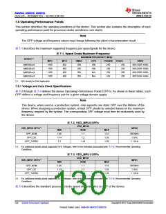
Overshoot = 20% of nominal
IO supply voltage
Tovershoot
Tperiod
Tundershoot
Undershoot = 20% of nominal
IO supply voltage
A. Tovershoot + Tundershoot < 20% of Tperiod
图7-1. IO Transient Voltage Ranges
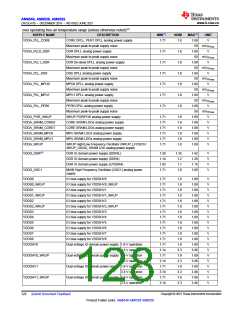
7.2 ESD Ratings
VALUE
UNIT
Human-body model (HBM), per ANSI/ESDA/JEDEC JS-001(1)
± 1000
Electrostatic discharge
(ESD)
V(ESD)
V
Charged-device model (CDM), per JEDEC specification ANSI/
ESDA/JEDEC JS-002(2)
± 250
(1) JEDEC document JEP155 states that 500-V HBM allows safe manufacturing with a standard ESD control process.
(2) JEDEC document JEP157 states that 250-V CDM allows safe manufacturing with a standard ESD control process.
Copyright © 2021 Texas Instruments Incorporated
126 Submit Document Feedback
Product Folder Links: AM6548 AM6528 AM6526

 TI [ TEXAS INSTRUMENTS ]