AM3359, AM3358, AM3357
AM3356, AM3354, AM3352
SPRS717F –OCTOBER 2011–REVISED APRIL 2013
www.ti.com
Revision History
NOTE: Page numbers for previous revisions may differ from page numbers in the current version.
Changes from Revision E (January 2013) to Revision F
Page
•
•
•
•
•
•
•
•
•
•
•
Changed device status to Production Data ....................................................................................... 1
Changed ARM speeds features list item .......................................................................................... 1
Changed MPU Subsystem speeds features list item ........................................................................... 1
Changed Features list item for DDR3 ............................................................................................. 1
Changed Features list item for DDR3L ........................................................................................... 1
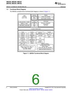
Changed Figure 1-1, AM335x Functional Block Diagram ...................................................................... 6
Changed Type value to I for Mode 2 (uart5_rxd) in Table 2-7, Ball Characteristics (ZCE and ZCZ Packages) ....... 37
Added Footnote (3) in Table 2-7, Ball Characteristics (ZCE and ZCZ Packages) ......................................... 49
Changed Footnote (4) in Table 2-7, Ball Characteristics (ZCE and ZCZ Packages) ...................................... 49
Added RTC_PORz Signal Name to Table 2-17, Miscellaneous/Miscellaneous Signals Description .................... 60
Deleted ESD-CDM (Charged-Device Model) Corner Terminals Parameter and changed MIN value for Latch-up
Performance Parameter in Table 3-1 ............................................................................................ 80
Changed DDR3, DDR3L value for OPP100 and deleted Footnote (3) in Table 3-2, VDD_CORE Operating
Performance Points for ZCZ Package with Device Revision Code "Blank" ................................................ 82
Deleted OPP50 row from Table 3-3, VDD_MPU Operating Performance Points for ZCZ Package with Device
Revision Code "Blank" ............................................................................................................. 82
Added Table 3-4, Valid Combinations of VDD_CORE and VDD_MPU Operating Performance Points for ZCZ
Package with Device Revision Code "Blank" ................................................................................... 82
Changed DDR3, DDR3L value for OPP100, deleted Footnote (4) and deleted OPP50 row from Table 3-5,
VDD_CORE Operating Performance Points for ZCE Package with Device Revision Code "Blank" .................... 83
Changed DDR3, DDR3L value for OPP100 and deleted Footnote (3) in Table 3-6, VDD_CORE Operating
Performance Points for ZCZ Package with Device Revision Code "A" or Newer ......................................... 84
Changed Table 3-7, VDD_MPU Operating Performance Points for ZCZ Package with Device Revision Code "A"
or Newer ............................................................................................................................. 84
Added Table 3-8, Valid Combinations of VDD_CORE and VDD_MPU Operating Performance Points for ZCZ
Package with Device Revision Code "A" or Newer ............................................................................ 84
Changed DDR3, DDR3L value for OPP100 and deleted Footnote (4) in Table 3-9, VDD_CORE Operating
Performance Points for ZCE Package with Device Revision Code "A" or Newer ......................................... 85
Added VDD_MPU Nitro Description and MAX value in Table 3-10, Maximum Current Ratings at AM335x Power
Terminals ............................................................................................................................ 86
Changed MAX value for VDDS_DDR Supply in Table 3-10, Maximum Current Ratings at AM335x Power
Terminals ............................................................................................................................ 86
Added paragraphs in the POH section before and after Table 3-11, Reliability Data ..................................... 87
Added Operating Condition Nitro to Table 3-11, Reliability Data ............................................................ 87
Added MIN, NOM, and MAX for VDD_MPU Nitro mode; deleted values from USB0_ID and USB1_ID; added
Footnote (7) in Table 3-12, Recommended Operating Conditions .......................................................... 87
Changed VOH, VOL, II and IOZ Parameter values in Table 3-13, DC Electrical Characteristics Over Recommended
Ranges of Supply Voltage and Operating Temperature ...................................................................... 90
Deleted TYP value for CVDDS_DDR Parameter in Table 3-15, Power-Supply Decoupling Capacitor Characteristics ... 94
Changed second paragraph in Section 4.2.2.3, OSC1 Internal Oscillator Clock Source ............................... 110
Changed second paragraph in Section 4.2.2.4, OSC1 LVCMOS Digital Clock Source ................................. 112
Added Section 5.4, DMTimer .................................................................................................... 117
Added OPP50 MIN values for all parameters and changed OPP100 MIN value for Parameters F13 and F22 in
Table 5-21, GPMC and NOR Flash Timing Requirements—Synchronous Mode ........................................ 126
Added OPP50 MIN and MAX values and changed MIN values of OPP100 Parameters F7 and F8 in Table 5-22,
GPMC and NOR Flash Switching Characteristics—Synchronous Mode .................................................. 127
Changed OPP50 MIN and MAX Parameter values in Table 5-26, GPMC and NOR Flash Switching
•
•
•
•
•
•
•
•
•
•
•
•
•
•
•
•
•
•
•
•
•
•
Characteristics—Asynchronous Mode ......................................................................................... 136
Changed OPP50 MIN and MAX Parameter values in Table 5-30, GPMC and NAND Flash Switching
Characteristics—Asynchronous Mode ......................................................................................... 145
Changed MIN value for Parameter 1 in Table 5-56, Switching Characteristics for DDR3 Memory Interface ........ 170
Added Conditions to Parameter 1 and deleted Footnote in Table 5-58, Compatible JEDEC DDR3 Devices (Per
Interface) ........................................................................................................................... 174
Changed Footnote (12) in Table 5-66, CK and ADDR_CTRL Routing Specification .................................... 187
Changed Footnote (11) in Table 5-67, DQS[x] and DQ[x] Routing Specification ........................................ 188
•
•
•
•
8
Contents
Copyright © 2011–2013, Texas Instruments Incorporated
Submit Documentation Feedback
Product Folder Links: AM3359 AM3358 AM3357 AM3356 AM3354 AM3352

 TI [ TEXAS INSTRUMENTS ]