ADS1274
ADS1278
www.ti.com
SBAS367F –JUNE 2007–REVISED FEBRUARY 2011
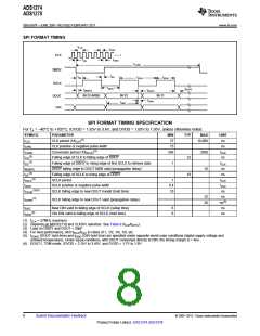
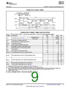
FRAME-SYNC FORMAT TIMING
tCPW
tCLK
CLK
tCPW
tCS
tFRAME
tFPW
tFPW
FSYNC
SCLK
DOUT
DIN
tFS
tSCLK
tSPW
tSF
tSPW
tMSBPD
Bit 23 (MSB)
tDOPD
tDOHD
Bit 21
Bit 22
tDIST
tDIHD
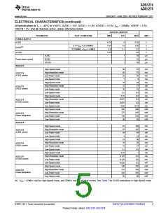
FRAME-SYNC FORMAT TIMING SPECIFICATION
For TA = –40°C to +105°C, IOVDD = 1.65V to 3.6V, and DVDD = 1.65V to 2.2V, unless otherwise noted.
SYMBOL PARAMETER
MIN
27
TYP
MAX
10,000
10,000
UNIT
ns
High-Speed mode
Other modes
tCLK
CLK period (1/fCLK) (see Table 7)
37
ns
tCPW
tCS
CLK positive or negative pulse width
11
ns
Falling edge of CLK to falling edge of SCLK
–0.25
256
1
0.25
tCLK
tCLK
tSCLK
ns
(1)
tFRAME
tFPW
tFS
Frame period (1/fDATA
)
2560
FSYNC positive or negative pulse width
Rising edge of FSYNC to rising edge of SCLK
Rising edge of SCLK to rising edge of FSYNC
SCLK period(2)
5
tSF
5
ns
tSCLK
tSPW
1
tCLK
tCLK
ns
SCLK positive or negative pulse width
0.4
10
(3)(4)
tDOHD
SCLK falling edge to old DOUT invalid (hold time)
31
21
25
31
21
25
ns
(4)
tDOPD
SCLK falling edge to new DOUT valid (propagation delay)
ns(5)
ns(6)
ns
ns(5)
ns(6)
ns
tMSBPD
FSYNC rising edge to DOUT MSB valid (propagation delay)
tDIST
New DIN valid to falling edge of SCLK (setup time)
Old DIN valid to falling edge of SCLK (hold time)
6
6
(3)
tDIHD
ns
(1) Depends on MODE[1:0] and CLKDIV selection. See Table 8 (fCLK/fDATA).
(2) SCLK must be continuously running and limited to ratios of 1, 1/2, 1/4, and 1/8 of fCLK
.
(3) tDOHD (DOUT hold time) and tDIHD (DIN hold time) are specified under opposite worst-case conditions (digital supply voltage and
ambient temperature). Under equal conditions, with DOUT connected directly to DIN, the timing margin is > 4ns.
(4) Load on DOUT = 20pF.
(5) DOUT1, TDM mode, IOVDD = 3.15V to 3.45V, and DVDD = 2V to 2.2V.
(6) DOUT1, TDM mode, IOVDD = 3.15V to 3.45V, and DVDD = 1.7V to 1.9V.
© 2007–2011, Texas Instruments Incorporated
Submit Documentation Feedback
9
Product Folder Link(s): ADS1274 ADS1278

 TI [ TEXAS INSTRUMENTS ]