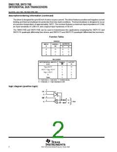
SN65176B, SN75176B
DIFFERENTIAL BUS TRANSCEIVERS
SLLS101D – JULY 1985 – REVISED APRIL 2003
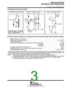
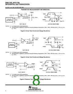
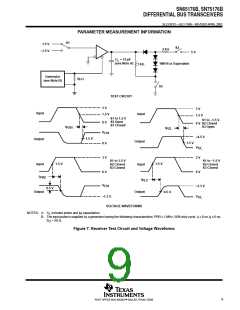
schematics of inputs and outputs
EQUIVALENT OF EACH INPUT
TYPICAL OF A AND B I/O PORTS
TYPICAL OF RECEIVER OUTPUT
V
V
CC
CC
V
CC
85 Ω
NOM
R
(eq)
960 Ω
NOM
16.8 kΩ
NOM
Input
960 Ω
NOM
Output
GND
Driver input: R
= 3 kΩ NOM
)= 8 kΩ NOM
Input/Output
Port
(eq)
Enable inputs: R
(eq
R
= Equivalent Resistor
(eq)
†
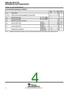
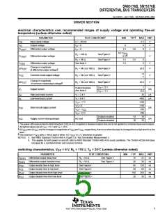
absolute maximum ratings over operating free-air temperature range (unless otherwise noted)
Supply voltage, V
(see Note 1) . . . . . . . . . . . . . . . . . . . . . . . . . . . . . . . . . . . . . . . . . . . . . . . . . . . . . . . . . . . . . 7 V
CC
Voltage range at any bus terminal . . . . . . . . . . . . . . . . . . . . . . . . . . . . . . . . . . . . . . . . . . . . . . . . . . . . –10 V to 15 V
Enable input voltage, V . . . . . . . . . . . . . . . . . . . . . . . . . . . . . . . . . . . . . . . . . . . . . . . . . . . . . . . . . . . . . . . . . . . . 5.5 V
I
Package thermal impedance, θ (see Notes 2 and 3): D package . . . . . . . . . . . . . . . . . . . . . . . . . . . . 97°C/W
JA
P package . . . . . . . . . . . . . . . . . . . . . . . . . . . . 85°C/W
PS package . . . . . . . . . . . . . . . . . . . . . . . . . . . 95°C/W
Operating virtual junction temperature, T . . . . . . . . . . . . . . . . . . . . . . . . . . . . . . . . . . . . . . . . . . . . . . . . . . . 150°C
J
Lead temperature 1,6 mm (1/16 inch) from case for 10 seconds . . . . . . . . . . . . . . . . . . . . . . . . . . . . . . . 260°C
Storage temperature range, T
. . . . . . . . . . . . . . . . . . . . . . . . . . . . . . . . . . . . . . . . . . . . . . . . . . . –65°C to 150°C
stg
†
Stresses beyond those listed under “absolute maximum ratings” may cause permanent damage to the device. These are stress ratings only, and
functional operation of the device at these or any other conditions beyond those indicated under “recommended operating conditions” is not
implied. Exposure to absolute-maximum-rated conditions for extended periods may affect device reliability.
NOTES: 1. All voltage values, except differential input/output bus voltage, are with respect to network ground terminal.
2. Maximum power dissipation is a function of T (max), θ , and T . The maximum allowable power dissipation at any allowable
J
JA
A
ambient temperature is P = (T (max) – T )/θ . Operating at the absolute maximum T of 150°C can affect reliability.
D
J
A
JA
J
3. The package thermal impedance is calculated in accordance with JESD 51-7.
3
POST OFFICE BOX 655303 • DALLAS, TEXAS 75265

 TI [ TEXAS INSTRUMENTS ]