SN65176B, SN75176B
DIFFERENTIAL BUS TRANSCEIVERS
SLLS101D – JULY 1985 – REVISED APRIL 2003
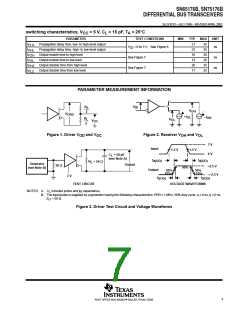
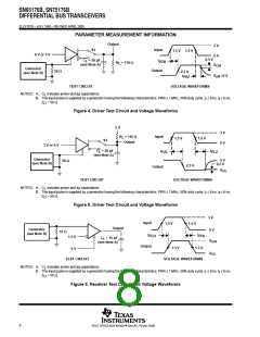
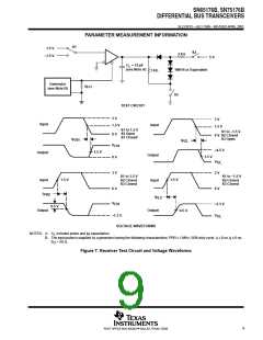
PARAMETER MEASUREMENT INFORMATION
Output
3 V
0 V
S1
Input
t
1.5 V 1.5 V
0 V or 3 V
0.5 V
C
= 50 pF
L
PZH
R
= 110 Ω
L
(see Note A)
V
OH
≈0 V
Generator
(see Note B)
Output
50 Ω
2.3 V
V
t
off
PHZ
TEST CIRCUIT
VOLTAGE WAVEFORMS
NOTES: A.
C includes probe and jig capacitance.
L
B. The input pulse is supplied by a generator having the following characteristics: PRR ≤ 1 MHz, 50% duty cycle, t ≤ 6 ns, t ≤ 6 ns,
r
f
Z
O
= 50 Ω.
Figure 4. Driver Test Circuit and Voltage Waveforms
5 V
3 V
0 V
R
= 110 Ω
Input
t
L
1.5 V
1.5 V
S1
Output
3 V or 0 V
C
= 50 pF
(see Note A)
t
L
PZL
PLZ
Generator
(see Note B)
5 V
0.5 V
50 Ω
2.3 V
Output
V
OL
TEST CIRCUIT
VOLTAGE WAVEFORMS
NOTES: A.
C includes probe and jig capacitance.
L
B. The input pulse is supplied by a generator having the following characteristics: PRR ≤ 1 MHz, 50% duty cycle, t ≤ 6 ns, t ≤ 6 ns,
r
f
Z
O
= 50 Ω.
Figure 5. Driver Test Circuit and Voltage Waveforms
3 V
0 V
Input
1.5 V
1.5 V
Output
= 15 pF
Generator
(see Note B)
51 Ω
t
t
PHL
PLH
1.5 V
0 V
C
L
V
OH
OL
(see Note A)
Output
1.3 V
1.3 V
V
TEST CIRCUIT
VOLTAGE WAVEFORMS
NOTES: A.
C includes probe and jig capacitance.
L
B. The input pulse is supplied by a generator having the following characteristics: PRR ≤ 1 MHz, 50% duty cycle, t ≤ 6 ns, t ≤ 6 ns,
r
f
Z
O
= 50 Ω.
Figure 6. Receiver Test Circuit and Voltage Waveforms
8
POST OFFICE BOX 655303 • DALLAS, TEXAS 75265

 TI [ TEXAS INSTRUMENTS ]