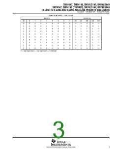
ꢀ
ꢁ
ꢅ
ꢔ
ꢂ
ꢃ
ꢇ
ꢃ
ꢄ
ꢐ
ꢄ
ꢃ
ꢈ
ꢃ
ꢇ
ꢅ
ꢆ
ꢉ
ꢑ
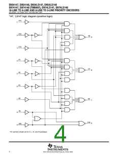
ꢀ
ꢁ
ꢌ
ꢒ
ꢂ
ꢍ
ꢃ
ꢍ
ꢕ
ꢄ
ꢎ
ꢃ
ꢅ
ꢋ
ꢇ
ꢆ
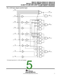
ꢀ
ꢀ
ꢑ
ꢁ
ꢂ
ꢃ
ꢗ
ꢃ
ꢈ
ꢈ
ꢀ
ꢀ
ꢄ
ꢗ
ꢄ
ꢃ
ꢃ
ꢅ
ꢘ
ꢅ
ꢆ
ꢆ
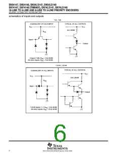
ꢀ
ꢀ
ꢁ
ꢁ
ꢙ
ꢂ
ꢅ
ꢒ
ꢃ
ꢃ
ꢈ
ꢈ
ꢔ
ꢀ
ꢀ
ꢑ
ꢄ
ꢄ
ꢗ
ꢃ
ꢃ
ꢀ
ꢇ
ꢇ
ꢀ
ꢁ
ꢅ
ꢃ
ꢄ
ꢃ
ꢅ
ꢆ
ꢀ
ꢁ
ꢊ
ꢋ
ꢏ
ꢆ
ꢁ
ꢅ
ꢄ
ꢎ
ꢐ
ꢈꢋ
ꢁ
ꢑ
ꢊ ꢒ
ꢃ
ꢐ
ꢈ
ꢋ
ꢁ
ꢑ
ꢓ
ꢁ
ꢋ
ꢁ
ꢊ
ꢐ
ꢈ
ꢁ
ꢖ
ꢋ
ꢒ
ꢋ
ꢊ
ꢑ
ꢁ
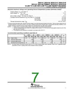
SDLS053B − OCTOBER 1976 − REVISED MAY 2004
†
absolute maximum ratings over operating free-air temperature (unless otherwise noted)
Supply voltage, V
(see Note 1) . . . . . . . . . . . . . . . . . . . . . . . . . . . . . . . . . . . . . . . . . . . . . . . . . . . . . . . . . . . . . 7 V
CC
Input voltage, V : ’147, ’148 . . . . . . . . . . . . . . . . . . . . . . . . . . . . . . . . . . . . . . . . . . . . . . . . . . . . . . . . . . . . . . . 5.5 V
I
’LS147, ’LS148 . . . . . . . . . . . . . . . . . . . . . . . . . . . . . . . . . . . . . . . . . . . . . . . . . . . . . . . . . . . . 7 V
Inter-emitter voltage: ’148 only (see Note 2) . . . . . . . . . . . . . . . . . . . . . . . . . . . . . . . . . . . . . . . . . . . . . . . . . . 5.5 V
Package thermal impedance θ (see Note 3): D package . . . . . . . . . . . . . . . . . . . . . . . . . . . . . . . . . . . 73°C/W
JA
N package . . . . . . . . . . . . . . . . . . . . . . . . . . . . . . . . . . . 67°C/W
NS package . . . . . . . . . . . . . . . . . . . . . . . . . . . . . . . . . . 64°C/W
. . . . . . . . . . . . . . . . . . . . . . . . . . . . . . . . . . . . . . . . . . . . . . . . . . . −65°C to 150°C
Storage temperature range, T
stg
†
Stresses beyond those listed under “absolute maximum ratings” may cause permanent damage to the device. These are stress ratings only, and
functional operation of the device at these or any other conditions beyond those indicated under “recommended operating conditions” is not
implied. Exposure to absolute-maximum-rated conditions for extended periods may affect device reliability.
NOTES: 1. Voltage values, except inter-emitter voltage, are with respect to the network ground terminal.
2. This is the voltage between two emitters of a multiple-emitter transistor. For ’148 circuits, this rating applies between any two of the
eight data lines, 0 through 7.
3. The package thermal impedance is calculated in accordance with JESD 51-7.
recommended operating conditions (see Note 4)
SN54’
SN74’
SN54LS’
SN74LS’
UNIT
MIN NOM MAX
MIN NOM MAX
MIN NOM MAX
MIN NOM MAX
V
Supply voltage
4.5
5
5.5 4.75
−800
5
5.25
−800
16
4.5
5
5.5 4.75
−400
5
5.25
−400
8
V
CC
OH
OL
I
I
High-level output current
Low-level output current
Operating free-air temperature
µA
mA
°C
16
4
T
A
−55
125
0
70
−55
125
0
70
NOTE 4: All unused inputs of the device must be held at V
or GND to ensure proper device operation. Refer to the TI application report,
CC
Implications of Slow or Floating CMOS Inputs, literature number SCBA004.
7
POST OFFICE BOX 655303 • DALLAS, TEXAS 75265

 TI [ TEXAS INSTRUMENTS ]