SN74AVC16646
16-BIT BUS TRANSCEIVER AND REGISTER
WITH 3-STATE OUTPUTS
www.ti.com
SCES181F–DECEMBER 1998–REVISED JUNE 2005
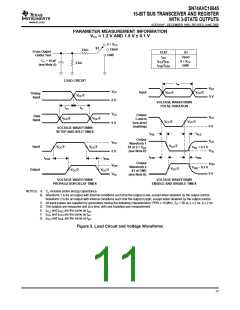
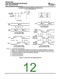
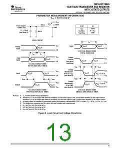
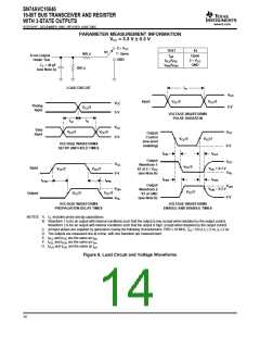
PARAMETER MEASUREMENT INFORMATION
VCC = 1.8 V ± 0.15 V
2 × V
CC
S1
Open
GND
1 kΩ
From Output
Under Test
TEST
S1
t
pd
Open
C = 30 pF
(see Note A)
L
t
/t
/t
2 × V
CC
GND
PLZ PZL
1 kΩ
t
PHZ PZH
LOAD CIRCUIT
t
w
V
CC
V
CC
V /2
CC
V /2
CC
Input
Timing
Input
V
/2
CC
0 V
0 V
VOLTAGE WAVEFORMS
PULSE DURATION
t
su
t
h
V
CC
Output
Control
(low-level
enabling)
Data
Input
V
CC
V
/2
CC
V /2
CC
V /2
CC
V /2
CC
0 V
0 V
VOLTAGE WAVEFORMS
SETUP AND HOLD TIMES
t
t
PLZ
PZL
Output
Waveform 1
V
CC
V
CC
V /2
CC
Input
V /2
CC
V /2
CC
S1 at 2 × V
V
OL
+ 0.15 V
CC
V
OL
(see Note B)
0 V
t
t
PHZ
PZH
t
t
PLH
PHL
Output
Waveform 2
S1 at GND
V
OH
V
V
OH
V
OH
− 0.15 V
V /2
CC
Output
V /2
CC
V /2
CC
0 V
OL
(see Note B)
VOLTAGE WAVEFORMS
PROPAGATION DELAY TIMES
VOLTAGE WAVEFORMS
ENABLE AND DISABLE TIMES
NOTES: A. C includes probe and jig capacitance.
L
B. Waveform 1 is for an output with internal conditions such that the output is low, except when disabled by the output control.
Waveform 2 is for an output with internal conditions such that the output is high, except when disabled by the output control.
C. All input pulses are supplied by generators having the following characteristics: PRR ≤ 10 MHz, Z = 50 Ω, t ≤ 2 ns, t ≤ 2 ns.
O
r
f
D. The outputs are measured one at a time, with one transition per measurement.
E.
F.
G.
t
t
t
and t
and t
and t
are the same as t
.
dis
.
PLZ
PZL
PLH
PHZ
are the same as t
PZH
en
are the same as t .
PHL pd
Figure 4. Load Circuit and Voltage Waveforms
12

 TI [ TEXAS INSTRUMENTS ]