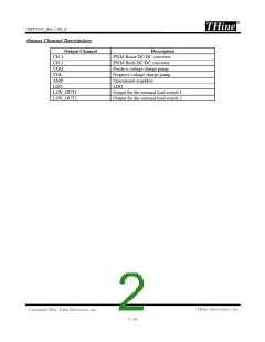
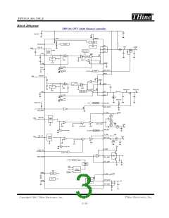
THV3543_Rev.1.00_E
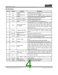
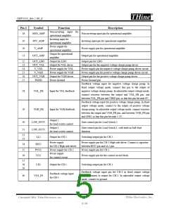
Pin #
Symbol
Function
Nonꢀinverting input for
operational amplifier
Inverting input for
operational amplifier
Power supply for
Description
18
NON_AMP
Nonꢀinverting input pin for operational amplifier.
19
20
21
INV_AMP
V_AMP
Inverting input pin for operational amplifier.
Power supply pin for operational amplifier.
Output pin for operational amplifier.
operational amplifier
Output for operational
amplifier
OUT_AMP
22
23
24
25
26
27
OUT_LDO
OUT_VGL
V_VGL
Output for LDO
Output pin for LDO.
Output for VGL driver
Power supply for VGL
Power supply for VGH
Output for VGH driver
Power Ground
Output pin for the negative voltage charge pump driver.
Power supply pin for negative voltage charge pump driver circuit.
Power supply pin for positive voltage charge pump driver circuit.
Output pin for the positive voltage charge pump driver.
Power Ground pin.
V_VGH
OUT_VGH
PGND
Feedback voltage input for negative voltage charge pump. In
fixed output voltage mode, connect this pin to the output of
negative voltage charge pump. In adjustable output voltage mode,
connect resistors between the output and VGL_FB pin, and
between VGL_FB pin and VREF pin, so that this pin become 0V.
Feedback voltage input for positive voltage charge pump. In fixed
output voltage mode, connect to the output of positive voltage
charge pump. In adjustable output voltage mode, connect resistors
between the output and VGH_FB pin, and between VGH_FB pin
and GND, so that this pin become 1.2V.
28
29
VGL_FB
VGH_FB
Input for VGL feedback
Input for VGH feedback
Output 2
30
31
LSW_OUT2
LSW_OUT1
LL2
Gate control pin for Load Switch 2.
for load switch control
Output 1
Gate control pin for Load Switch 1, with builtꢀin Soft Start
function.
for load switch control
32
33
Output for CHꢀ2
Switching output pin for CHꢀ2.
Power supply
Power supply pin for CHꢀ2 High side driver. Connect a capacitor
between BST2 pin and LL2 pin.
34
35
36
BST2
PVCC
VCC
for CHꢀ2 High side driver
Power supply for CHꢀ2
Power supply
Power supply pin for CHꢀ2.
Power supply pin for the control circuit block.
for control circuit
37
38
39
LX1
Output for CHꢀ1
Switching output pin for CHꢀ1.
Feedback voltage input pin for CHꢀ1 in fixed output voltage
mode. Connect to output for CHꢀ1. In adjustable output voltage
mode, connect to ground.
Feedback voltage input
for CHꢀ1
40
VO1_IN
THine Electronics, Inc.
Copyright© 2011 THine Electronics, Inc.
5/19

 THINE [ THINE ELECTRONICS, INC. ]