THV3543_Rev.1.00_E
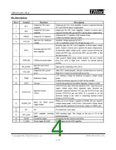
Pin Descriptions
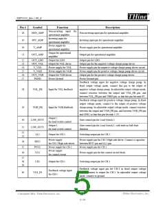
Pin #
Symbol
Function
Output for CHꢀ2 error
amplifier
Description
Output pin for CHꢀ2 error amplifier. Connect a capacitor between
PC2 and GND for phase compensation.
1
PC2
Output for CHꢀ1 error
amplifier
Output pin for CHꢀ1 error amplifier. Connect a resistor and a
capacitor between FB1 pin and INV1 pin for phase compensation.
Output pin for 5V regulator of the control circuit.
Connect an external capacitor (10ꢁF).
2
3
4
FB1
VREG5
VO2_IN
Output for 5V regulator
Input for CHꢀ2 feedback
voltage
Feedback voltage input pin for CHꢀ2.
CHꢀ2 is controlled so that VO2_IN pin becomes 3.3V.
Inverting input for CHꢀ1 error amplifier. In fixed output voltage
mode, connect a resistor and a capacitor for phase compensation.
In adjustable output voltage mode, connect resistors between the
output and INV1 pin, and between INV1 pin and GND, so that
this pin become 1.2V.
Inverting input for CHꢀ1
error amplifier
5
6
INV1
After positive charge pump started properly, this pin switches
from Low level to High level. Connect an external pullꢀup
resistor.
VGH_OK
VGH power good output
Input for load switch
control
7
8
PG_LOGIC
VO2_OK
Input pin for controlling LSW_OUT2.
Output for CHꢀ2 power
good
After CHꢀ2 started properly, this pin switches from Low level to
High level. Connect an external pullꢀup resistor.
1.2V reference voltage for feedback of negative voltage charge
pump.
9
VREF
TEST
Reference voltage
Test pin
Connect an external capacitor (0.01ꢁF) for the stability.
Used for the production test before shipment. Connect to GND.
SYSUVLO pin shuts down the operation of IC, when the power
supply voltage drops below regulated value. Resistors are
internally connected between VCC pin and SYSUVLO pin, and
between SYSUVLO pin and GND. It is possible to set the
detection voltage at any value by connecting external resister
divider to SYSUVLO pin.
10
Input for System
UVLO
11
SYSUVLO
When Low level voltage is applied to PANEL_EN pin, negative
voltage charge pump, Load Switch 1 and positive voltage charge
pump stop their operations. If not in use, connect to VREG5 pin.
Input for Panel power
supply enable
12
PANEL_EN
13
14
NC
NC
No connection. Leave open.
LDO amplifier inverting LDO inverting input. The voltage on this pin is 1.2V in the
15
INV_LDO
input
normal operation.
16
17
SGND
Ground for signal
Power supply for LDO
Ground pin for the control circuit block.
Power supply pin for LDO amplifier.
V_LDO
THine Electronics, Inc.
Copyright© 2011 THine Electronics, Inc.
4/19

 THINE [ THINE ELECTRONICS, INC. ]