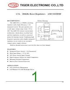
AMC3202DMF
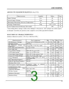
ABSOLUTE MAXIMUM RATINGS (Ta=25°C)
Characteristic
Symbol
Value
30
Unit
V
Input Voltage
Vcc
Vsw
Tj
Switch Input Voltage,
40
V
Maximum Operating Junction Temperature
Storage Temperature
150
°C
°C
°C
Tstg
-65~ +150
260
Lead Temperature(Soldering,10seconds)
* Exceeding these ratings could cause damage to the device. All voltages are with respect
to Ground. Currents are positive into, negative out of the specified terminal.
ELECTRICAL CHARACTERISTICS
(Unless otherwise noted: 2.7V<Vcc<30V,Ta=25℃ )
Characteristics
FB Reference Voltage
FB Input Current
Test conditions
VC O M P tied to FB;Measure at FB
FB=VR E F
Min
1.246
-1.0
Typ Max Unit
V
1.276 1.300
0.1 1.0
0.01 0.03
µA
FB Reference Voltage Line
%/V
VC O M P =FB, 2.7V<Vcc<30V
Regulation
Error Amp Transconductance
Error Amp Gain
IV C O M P =±25µA
uMho
V/V
µA
µA
V
300
200
25
200
1.5
550
500
50
625 1500
1.7 1.9
800
*
VC O M P Source Current
VC O M P Sink Current
FB=1.0V, VC O M P =1.25V
FB=1.5V, VC O M P =1.25V
FB=1.0V, VC O M P sources 25µA
FB=1.5V, VC O M P sinks 25µA
90
VC O M P High Clamp Voltage
VC O M P Low Clamp Voltage
V
0.25
0.50 0.65
Reduce VC O M P from 1.5V until
VC O M P Threshold
V
0.75
1.05 1.30
switching stops
Base Operating Frequency
Reduced Operating Frequency
Maximim Duty Cycle
FB=1V
FB=0V
kHZ
kHZ
%
230
30
90
280
52
94
310
120
Frequency drops to reduced
operating frequency
FB Frequency Shift Threshold
V
kHZ
V
0.36
320
2.5
0.40 0.44
500
Synchronization range
Synchronization
Pulse
Rise time=20ns
Transition Threshold
EN=0V
-15
-3.0
EN Bias Current
Shutdown Threshold
Shutdown Delay
µA
V
EN=3.0V
3.0
8.0
0.50
0.85 1.20
2.7V≤Vcc≤12V
12V≤Vcc≤30V
12
80
350
µS
12
36
200
3/6

 TGS [ Tiger Electronic Co.,Ltd ]