AMC3202DMF
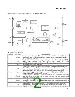
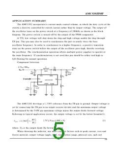
BLOCK DIAGRAM AND PI N CONFIGURATION
PIN DESCRIPTION
Pin No. Pin Name
Pin Function
Loop compensation pin. This pin is the output of the error amplifier and
is used for loop compensation.Loop compensation can be implemented
by a simple RC network.
1
COMP
Feedback pin. Sense the output voltage and referenced to 1.276V.
2
3
FB
When
the
voltage
at
this
pin
falls
below
0.4V,chip
switching-frequency reduces to a much lower frequency.
No connection.Keep floating.
NC
Enable pin. A TTL low will shut down the chip and high enable the
chip. This pin may also be used to synchronize the part to nearly
twice the base frequency. If synchronization is not used, this pin
should be either tied high or left floating for normal operation.
Input power supply pin. Supply power to the IC and should have a
bypass capacitor connected to AGND
4
EN
5
6
Vcc
Analog ground. Provide a clean ground for the controller circuitry
and should not be in the path of large currents.This pin is connected
to the IC substrate.
AGND
Power ground. This pin is the ground connection for the emitter of
the power switching transistor.Connection to a good ground plane is
essential.
High current switch pin. Connect to the collector of the internal
power switch. The open voltage across the power switch can be as
high as 40V. To minimize radiation, use a trace as short as practical.
7
8
PGND
Vsw
2/6

 TGS [ Tiger Electronic Co.,Ltd ]