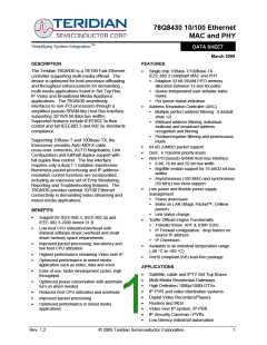
78Q8430 Data Sheet
DS_8430_001
Table of Contents
1
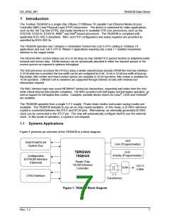
Introduction .........................................................................................................................................7
1.1 Systems Applications...................................................................................................................7
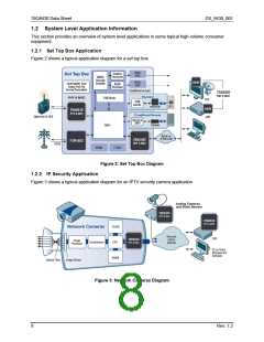
1.2 System Level Application Information..........................................................................................8
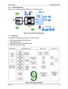
1.2.1 Set Top Box Application ..................................................................................................8
1.2.2 IP Security Application.....................................................................................................8
1.2.3 IP PBX Application...........................................................................................................9
1.3 Overview......................................................................................................................................9
1.4 Application Environments ..........................................................................................................10
1.5 Supply Voltages.........................................................................................................................10
1.6 Power Management...................................................................................................................10
2
3
Pinout.................................................................................................................................................11
Pin Description..................................................................................................................................12
3.1 Pin Legend.................................................................................................................................12
3.2 Pin Descriptions.........................................................................................................................12
3.2.1 Clock Pins......................................................................................................................12
3.2.2 Media Dependent Interface (MDI) Pins .........................................................................13
3.2.3 LED Display (PHY) Pins ................................................................................................13
3.2.4 EEPROM Pins ...............................................................................................................13
3.2.5 GBI Data Pins ................................................................................................................14
3.2.6 GBI Address Pins ..........................................................................................................15
3.2.7 GBI Control Pins............................................................................................................15
3.2.8 Mode Pins......................................................................................................................16
3.2.9 JTAG Pins......................................................................................................................16
3.2.10 Power Pins.....................................................................................................................17
4
Electrical Specification.....................................................................................................................18
4.1 Absolute Maximum Ratings.......................................................................................................18
4.2 Recommended Operation Conditions........................................................................................18
4.3 DC Characteristics.....................................................................................................................18
4.4 Digital I/O Characteristics ..........................................................................................................19
4.5 Analog Electrical Characteristics ...............................................................................................19
4.5.1 100Base-TX Transmitter................................................................................................19
4.5.2 100Base-TX Transmitter (Informative) ..........................................................................19
4.5.3 100Base-TX Receiver....................................................................................................20
4.5.4 10Base-T Transmitter....................................................................................................20
4.5.5 10Base-T Transmitter (Informative)...............................................................................20
4.5.6 10Base-T Receiver........................................................................................................21
5
6
Host Interface Timing Specification................................................................................................22
5.1 Host Interface.............................................................................................................................22
5.1.1 Synchronous Mode Timing............................................................................................23
5.1.2 Bus Clock Timing...........................................................................................................24
5.1.3 Reset Timing..................................................................................................................24
Functional Description.....................................................................................................................25
6.1 Internal Block Diagrams.............................................................................................................25
6.1.1 Internal Digital Block......................................................................................................25
6.1.2 Internal PHY...................................................................................................................25
6.2 Data Queuing.............................................................................................................................26
6.3 Host Interface.............................................................................................................................27
6.3.1 Reading Receive Data...................................................................................................27
6.3.2 Writing Transmit Data....................................................................................................27
6.3.3 DMA Slave Mode Access ..............................................................................................29
6.4 Snoop Mode Access..................................................................................................................29
6.5 Water Marking............................................................................................................................30
6.5.1 Interrupt Watermark.......................................................................................................30
2
Teridian Proprietary and Confidential
Rev. 1.2

 TERIDIAN [ TERIDIAN SEMICONDUCTOR CORPORATION ]