73S1215F Data Sheet
DS_1215F_003
Parameter
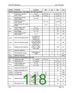
Interface Requirements – Data Signals: I/O, AUX1 and AUX2
Symbol
Condition
Min
Typ.
Max
Unit
IOH =0
0.9 * VCC
0.75 VCC
VCC+0.1
VCC+0.1
V
V
Output level, high (I/O,
AUX1, AUX2)
VOH
IOH = -40μA
Output level, low (I/O,
AUX1, AUX2)
0.15 *VCC
VCC+0.30
0.2 * VCC
VOL
VIH
VIL
IOL=1mA
V
V
V
Input level, high (I/O,
AUX1, AUX2)
0.6 * VCC
-0.15
Input level, low (I/O, AUX1,
AUX2)
IOL = 0
0.1
0.3
10
V
V
Output voltage when
outside of session
VINACT
IOL = 1mA
VIH = VCC
ILEAK
IIL
Input leakage
μA
Input current, low (I/O,
AUX1, AUX2)
VIL = 0
0.65
mA
For output low,
shorted to VCC
through 33Ω
ISHORTL
ISHORTH
tR, tF
Short circuit output current
Short circuit output current
Output rise time, fall times
15
mA
For output high,
shorted to ground
through 33Ω
15
mA
ns
For I/O, AUX1,
AUX2, CL = 80pF,
10% to 90%.
100
tIR, tIF
RPU
Input rise, fall times
Internal pull-up resistor
Maximum data rate
1
14
1
μs
kΩ
Output stable for
>200ns
8
11
FDMAX
MHz
Reset and Clock for Card Interface, RST, CLK
VOH
VOL
Output level, high
Output level, low
0.9 * VCC
0
VCC
0.15 *VCC
0.1
V
V
V
V
IOH =-200μA
IOL=200μA
IOL = 0
Output voltage when
outside of session
VINACT
IOL = 1mA
0.3
IRST_LIM
ICLK_LIM
Output current limit, RST
Output current limit, CLK
30
70
mA
V/ns
V/ns
CLKSR3V CLK slew rate
CLKSR5V CLK slew rate
VCC = 3V
VCC = 5V
0.3
0.5
CL = 35pF for CLK,
10% to 90%
8
ns
ns
tR, tF
Output rise time, fall time
CL = 200pF for RST,
10% to 90%
100
CL =35pF,
Duty cycle for CLK
45
55
%
δ
FCLK ≤ 20MHz
118
Rev. 1.4

 TERIDIAN [ TERIDIAN SEMICONDUCTOR CORPORATION ]