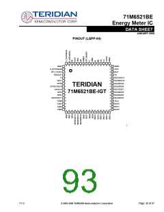
71M6521BE
Energy Meter IC
DATA SHEET
JANUARY 2008
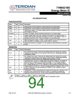
PIN DESCRIPTIONS
Power/Ground Pins:
Name
Type Circuit Description
GNDA
GNDD
P
P
--
--
Analog ground: This pin should be connected directly to the ground plane.
Digital ground: This pin should be connected directly to the ground plane.
Analog power supply: A 3.3V power supply should be connected to this pin, must be the
same voltage as V3P3SYS.
V3P3A
P
P
--
--
V3P3SYS
System 3.3V supply. This pin should be connected to a 3.3V power supply.
Auxiliary voltage output of the chip, controlled by the internal 3.3V selection switch. In
mission mode, this pin is internally connected to V3P3SYS. In BROWNOUT mode, it is
internally connected to VBAT. This pin is floating in LCD and sleep mode.
V3P3D
O
13
Battery backup power supply. A battery or super-capacitor is to be connected between
VBAT and GNDD. If no battery is used, connect VBAT to V3P3SYS.
VBAT
V2P5
P
12
10
Output of the internal 2.5V regulator. A 0.1µF capacitor to GNDA should be connected to
this pin.
O
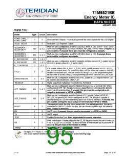
Analog Pins:
Name
Type
Circuit Description
Line Current Sense Inputs: These pins are voltage inputs to the internal A/D converter.
IA, IB
I
I
6
Typically, they are connected to the outputs of current sensors. Unused pins must be
connected to V3P3A.
Line Voltage Sense Inputs: These pins are voltage inputs to the internal A/D converter.
Typically, they are connected to the outputs of resistor dividers. Unused pins must be
connected to V3P3A or tied to the voltage sense input that is in use.
VA, VB
6
Comparator Input: This pin is a voltage input to the internal comparator. The voltage ap-
plied to the pin is compared to an internal BIAS voltage (1.6V). If the input voltage is
above the reference, the comparator output will be high (1). If the comparator output is
low, a voltage fault will occur. A 0.1µF capacitor to GNDA should be connected to this pin.
V1
I
7
Voltage Reference for the ADC. This pin is normally disabled by setting the VREF_CAL bit
in the I/O RAM and can be left unconnected. If enabled, a 0.1µF capacitor to GNDA
should be connected.
VREF
O
I
9
8
Crystal Inputs: A 32kHz crystal should be connected across these pins. Typically, a 27pF
capacitor is also connected from each pin to GNDA. It is important to minimize the
capacitance between these pins. See the crystal manufacturer datasheet for details.
XIN
XOUT
Pin types: P = Power, O = Output, I = Input, I/O = Input/Output
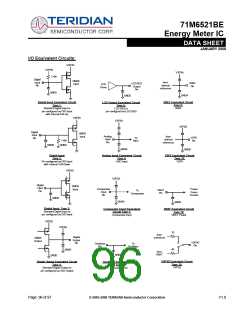
The circuit number denotes the equivalent circuit, as specified under “I/O Equivalent Circuits”.
Page: 94 of 97
© 2005-2008 TERIDIAN Semiconductor Corporation
V1.0

 TERIDIAN [ TERIDIAN SEMICONDUCTOR CORPORATION ]