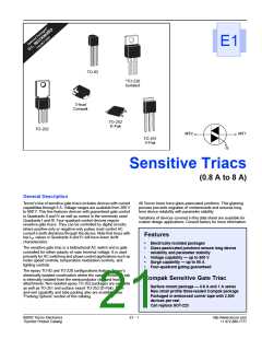
Sensitive Triacs
Data Sheets
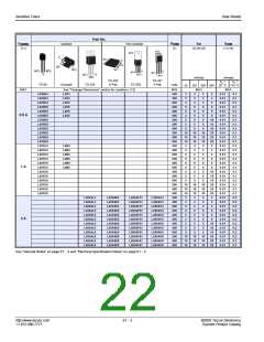
Part No.
I
V
I
I
DRM
(1) (14)
Isolated
Non-isolated
T(RMS)
(11)
DRM
(1)
GT
(3) (6)
MT2
MT2
G
MT2
MT1
G
MT1
G
MT1
MT2
MT2
TO-252
D-Pak
TO-251
V-Pak
mAmps
mAmps
QIV TC = 25 °C TC = 110 °C
MAX
TO-220
Volts
QI
QII
QIII
MAX
See “Package Dimensions” section for variations. (12)
MIN
200
400
600
200
400
600
200
400
600
200
400
600
200
400
600
MAX
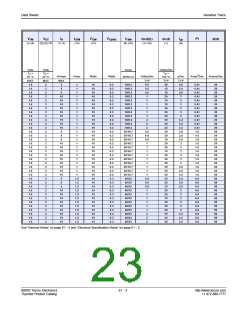
L2006L5
L2006D5
L4006D5
L6006D5
L2006D6
L4006D6
L6006D6
L2006D8
L4006D8
L6006D8
L2008D6
L4008D6
L6008D6
L2008D8
L4008D8
L6008D8
L2006V5
5
5
5
5
5
5
5
0.02
0.02
0.02
0.02
0.02
0.02
0.02
0.02
0.02
0.02
0.02
0.02
0.02
0.02
0.02
0.5
0.5
0.5
0.5
0.5
0.5
0.5
0.5
0.5
0.5
0.5
0.5
0.5
0.5
0.5
L4006L5
L6006L5
L2006L6
L4006L6
L6006L6
L2006L8
L4006L8
L6006L8
L2008L6
L4008L6
L6008L6
L2008L8
L4008L8
L6008L8
L4006V5
L6006V5
L2006V6
L4006V6
L6006V6
L2006V8
L4006V8
L6006V8
L2008V6
L4008V6
L6008V6
L2008V8
L4008V8
L6008V8
5
5
5
5
5
6 A
5
5
5
10
10
10
20
20
20
10
10
10
20
20
20
5
5
5
5
5
5
10
10
10
5
10
10
10
5
10
10
10
5
5
5
10
10
10
5
5
8 A
5
5
10
10
10
10
10
10
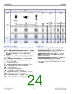
Specified Test Conditions
General Notes
di/dt — Maximum rate-of-change of on-state current; IGT = 50 mA with
•
•
•
All measurements are made with 60 Hz resistive load and at an
0.1 µs rise time
ambient temperature of +25 °C unless otherwise specified.
dv/dt — Critical rate-of-rise of off-state voltage at rated VDRM gate open
Operating temperature range (TJ) is -65 °C to +110 °C for TO-92
devices and -40 °C to 110 °C for all other devices.
Storage temperature range (TS) is -65 °C to +150 °C for TO-92
devices, -40 °C to +150 °C for TO-202 devices, and -40 °C to
+125 °C for TO-220 devices.
Lead solder temperature is a maximum of 230 °C for 10 seconds
maximum at a minimum of 1/16” (1.59 mm) from case.
The case or lead temperature (TC or TL) is measured as shown on
dimensional outline drawings. See “Package Dimensions” section
of this catalog.
dv/dt(c) — Critical rate-of-rise of commutation voltage at rated VDRM
and IT(RMS) commutating di/dt = 0.54 rated IT(RMS)/ms; gate
unenergized
2
I t — RMS surge (non-repetitive) on-state current for period of 8.3 ms
for fusing
•
•
I
I
— Peak off-state current, gate open; VDRM = max rated value
— DC gate trigger current in specific operating quadrants;
VD = 12 V dc; RL = 60 Ω
DRM
GT
I
I
I
I
— Peak gate trigger current
— Holding current gate open; initial on-state current = 100 mA dc
GTM
H
— RMS on-state current conduction angle of 360°
T(RMS)
— Peak one-cycle surge
TSM
P
P
— Average gate power dissipation
— Peak gate power dissipation; IGT ≤ IGTM
G(AV)
GM
t
— Gate controlled turn-on time; IGT = 50 mA with 0.1 µs rise time
gt
V
V
V
— Repetitive peak off-state/blocking voltage
— DC gate trigger voltage; VD = 12 V dc; RL = 60 Ω
— Peak on-state voltage at max rated RMS current
DRM
GT
TM
http://www.teccor.com
+1 972-580-7777
E1 - 4
©2002 Teccor Electronics
Thyristor Product Catalog

 TECCOR [ TECCOR ELECTRONICS ]