C2510Fx / CC2511Fx
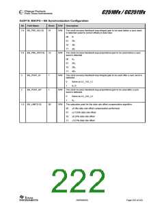
0xDF16: BSCFG – Bit Synchronization Configuration
Bit Field Name
Reset
R/W
Description
7:6 BS_PRE_KI[1:0]
01
R/W
The clock recovery feedback loop integral gain to be used before a sync word
is detected (used to correct offsets in data rate):
00
01
10
11
KI
2KI
3KI
4KI
5:4 BS_PRE_KP[1:0]
10
R/W
The clock recovery feedback loop proportional gain to be used before a sync
word is detected
00
01
10
11
KP
2KP
3KP
4KP
3
2
BS_POST_KI
BS_POST_KP
1
R/W
R/W
R/W
The clock recovery feedback loop integral gain to be used after a sync word is
detected.
0
1
Same as BS_PRE_KI
KI /2
1
The clock recovery feedback loop proportional gain to be used after a sync
word is detected.
0
1
Same as BS_PRE_KP
KP
1:0 BS_LIMIT[1:0]
00
The saturation point for the data rate offset compensation algorithm:
00
01
10
11
±0 (No data rate offset compensation performed)
±3.125% data rate offset
±6.25% data rate offset
±12.5% data rate offset
SWRS055D
Page 222 of 243

 TAOS [ TEXAS ADVANCED OPTOELECTRONIC SOLUTIONS ]