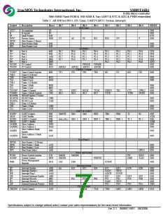
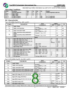
SyncMOS Technologies International, Inc.
SM89T16R1
8-Bits Micro-controller
With 64KB Flash ROM & 1KB RAM & Two UART & RTC & ADC & PWM embedded
2.5 tCLCL–5
-5
tMCS >0
tQVWX
tWHQX
9
9
Data valid to /WR transition
Data hold after /WR
ns
ns
tMCS =0
1.0 tCLCL -5
1.0 tCLCL -5
2.0 tCLCL -5
tMCS >0
tMCS =0
t
MCS >0
tRLAZ
8
/RD LOW to address float
0.5 tCLCL–5
10
ns
ns
tWHLH
8,9
/RD or /WR HIGH to ALE HIGH
0
t
MCS =0
1.0 tCLCL -5
1.0 tCLCL +5
tMCS >0
Notes:
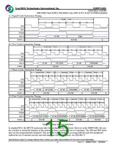
tMCS is time period related to the Stretch memory cycle selection. The following table shows the value of tMCS for each Stretch selection.
M2 M1 M0
MOVX Cycles
2 machine cycles
3 machine cycles
4 machine cycles
5 machine cycles
6 machine cycles
7 machine cycles
8 machine cycles
9 machine cycles
tMCS
0
0
0
0
1
1
1
1
0
0
1
1
0
0
1
1
0
1
0
1
0
1
0
1
0
4 tCLCL
8 tCLCL
12 tCLCL
16 tCLCL
20 tCLCL
24 tCLCL
28 tCLCL
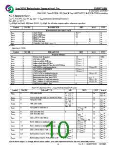
Parameter
Figure
Symbol
Min
Typ
Max
Unit
ns
Serial Port Clock Cycle Time
10
tXLXL
12 tCLCL
4 tCLCL
SM2=0,12 clocks per cycle
SM2=1,4 clocks per cycles
Output Data Setup to Clock Rising
SM2=0,12 clocks per cycle
SM2=1,4 clocks per cycles
Output Data Hold to Clock Rising
SM2=0,12 clocks per cycle
SM2=1,4 clocks per cycles
Input Data Hold to Clock Rising
SM2=0,12 clocks per cycle
SM2=1,4 clocks per cycles
ns
10
10
10
10
tQVXH
tXHQX
tXHDX
tXHDV
12 tCLCL
4 tCLCL
ns
ns
12 tCLCL
4 tCLCL
ns
ns
12 tCLCL
4 tCLCL
ns
ns
Clock Rising Edge to Input Data Valid
SM2=0,12 clocks per cycle
12 tCLCL
4 tCLCL
ns
ns
SM2=1,4 clocks per cycles
tCLCH
tCHCL
VIH1
0.8V
tCLCX
tCLCL
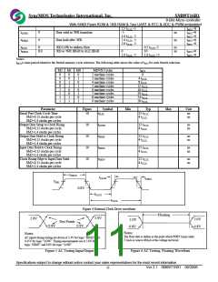
Figure 4 External Clock Drive waveform
Floating
2.0V
2.0V
2.0V
2.0V
0.8V
Test Points
0.8V
0.8V
0.8V
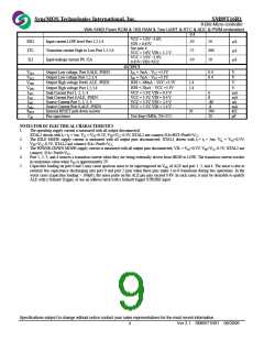
Notes:
Notes:
The float state is define as the point which PORT 0 pins sinks
AC inputs during testing are driven at 2.4V for logic “HIGH” and
0.45V for logic “LOW”. Timing measurements are at 2.0V for
logic “HIGH” and 0.8V for logic “LOW”
3.2mA or source 400µA at the voltage test level.
Figure 5 AC Testing Input/Output
Figure 6 AC Testing, Floating Waveform
Specifications subject to change without notice contact your sales representatives for the most recent information.
Ver 2.1 SM89T16R1 08/2006
11

 SYNCMOS [ SYNCMOS TECHNOLOGIES,INC ]