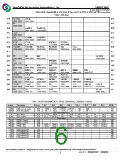
SyncMOS Technologies International, Inc.
SM89T16R1
8-Bits Micro-controller
With 64KB Flash ROM & 1KB RAM & Two UART & RTC & ADC & PWM embedded
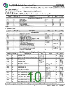
AC Characteristic
VCC=3.3V±10%, VSS=0V, tclk min = 1/ fmax(maximum operating frequency)
TA=-40℃ to +85℃
CL=100pF for Port0, ALE and /PSEN; CL=80pF for all other outputs unless otherwise specified.
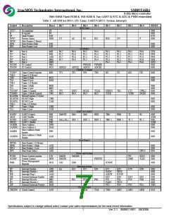
Symbol
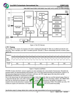
FIGURE
PARAMETER
MIN
MAX
UNIT
ns
External Clock drive into XTAL1
tCLCL
tCHCX
4
Xtal1 Period
62.5 (1)
-
4
4
4
4
4
Xtal1 HIGH time
Xtal1 LOW time
XTAL1 rise time
XTAL1 fall time
31
31
-
-
ns
ns
ns
ns
ns
tCLCX
-
tCLCH
15
15
-
tCHCL
-
tCYC
Controller cycle time = tCLCL / 4
5.2
NOTES:
1. Operating at 25MHz.
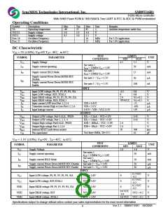
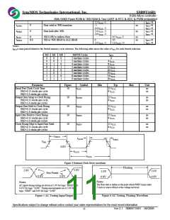
Symbol FIGURE
1/tCLCL
PARAMETER
Program Memory
MIN
MAX
UNIT
7
7
7
7
8
7
7
7
7
7
7
7
7
7
System clock frequency
3.0
16
MHz
ns
ns
ns
ns
ns
ns
ns
ns
ns
ns
ns
ns
ns
tLHLL
tAVLL
tLLAX
tLLAX
tLLIV
tLLPL
tPLPH
tPLIV
ALE pulse width
1.5 tCLCL -5
0.5 tCLCL -5
0.5 tCLCL -5
0.5 tCLCL -5
Address valid to ALE low
Address hold after ALE low
Address hold after ALE low for MOVX Write
ALE LOW to valid instruction in
ALE LOW to /PSEN LOW
2.5tCLCL-20
2.0tCLCL-20
0.5 tCLCL -5
2.0 tCLCL -5
/PSEN pulse width
/PSEN LOW to valid instruction in
Input instruction hold after /PSEN
Input instruction float after /PSEN
Port 0 Address to valid instruction in
Port 2 Address to valid instruction in
/PSEN low to address float
tPXIX
0
tPXIZ
tCLCL -5
tAVIV1
tAVIV2
tPLAZ
3.0tCLCL-20
3.5tCLCL-20
0
MOVX Characteristics Using Stretch Memory Cycles
Symbol
FIGURE
PARAMETER
ALE pulse width
MIN
MAX
UNIT Stretch
tLHLL2
8
1.5 tCLCL –5
2.0 tCLCL -5
ns
tMCS =0
t
MCS >0
tLLAX2
tRLRH
9
8
Address hold after ALE low for MOVX Write
/RD pulse width
0.5 tCLCL -5
2.0 tCLCL –5
tMCS -10
ns
ns
t
MCS =0
tMCS >0
tMCS =0
tWLWH
tRLDV
tRHDX
9
8
/WR pulse width
2.0 tCLCL –5
ns
ns
t
MCS -10
tMCS >0
/RD LOW to valid data in
2.0 tCLCL –20
tMCS =0
MCS >0
t
MCS -20
t
8
8
Data hold after /RD
Data float after /RD
0
ns
ns
tRHDZ
tCLCL –5
tMCS =0
MCS >0
tMCS =0
MCS >0
tMCS =0
MCS >0
2.0 tCLCL –5
2.5 tCLCL –5
t
tLLDV
tAVIV1
tAVIV2
tLLWL
tAVWL1
tAVDV2
8
ALE LOW to valid data in
ns
ns
ns
ns
ns
ns
t
MCS+2.0tCLCL –40
t
8
Port 0 Address to valid instruction in
Port 2 Address to valid instruction in
ALE LOW to /RD or /WR LOW
Port0 Address valid to /WR or /RD LOW
Port2 Address valid to /WR or /RD LOW
3.0 tCLCL-20
2.0 tCLCL –5
3.5 tCLCL-20
2.5 tCLCL –5
0.5 tCLCL+5
1.5 tCLCL+5
t
7,8
8,9
8,9
9
tMCS =0
t
t
MCS >0
MCS =0
0.5 tCLCL–5
1.5 tCLCL–5
tCLCL–5
tMCS >0
t
MCS =0
2.0 tCLCL–5
1.5tCLCL–5
tMCS >0
tMCS =0
Specifications subject to change without notice contact your sales representatives for the most recent information.
Ver 2.1 SM89T16R1 08/2006
10

 SYNCMOS [ SYNCMOS TECHNOLOGIES,INC ]