SM39A16M1
8-Bit Micro-controller
16KB with ISP Flash
& 1K+256B RAM embedded
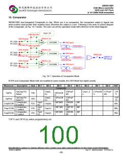
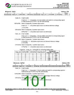
19. Comparator
SM39A16M1 had integrated Comparator in chip. When use it as comparator, the comparator output is logical one
when positive input greater than negative input, otherwise the output is a zero. Following is the work of a block diagram
of the comparator, as Fig. 19-1 shown. The user can set the operation mode with reference to the block diagram.
Vref 1.2V
SFR(C0PosVBG)
SFR(Hys0_En)
SFR(C0PosPad)
+
-
P2.1
P2.0
Level shifter
CMP0
SFR(Cmp0o)
SFR(Cmp0_En)
SFR(C1PosPad)
SFR(C1PosVBG)
SFR(CMF0)
SFR(CMF0MS)
SFR(Cmp1o)
SFR(Hys1_En)
+
P2.3
P2.2
Level shifter
CMP1
-
SFR(ECmpI)
SFR(Cmp1_En)
SFR(C2PosPad)
SFR(C2PosVBG)
CMP INT To
INT Circuirt
SFR(CMF1)
SFR(CMF1MS)
SFR(Cmp2o)
SFR(CMF2)
SFR(Hys2_En)
P2.5
P2.4
+
Level shifter
CMP2
-
SFR(Cmp2_En)
SFR(CMF2MS)
Fig. 19-1: Operation of Comparator Mode
If OPA and Comparator Mode both are enabled at same module, the OPA Mode has higher priority.
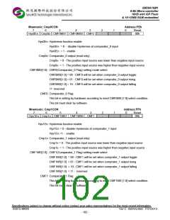
Mnemonic Description
Addr Bit 7
Bit 6
Bit 5
Bit 4
Bit 3
Bit 2
Bit 1
Bit 0
RST
Comparator
OpCmp Pin
Cmp0_
En
C0PosP
AD
Cmp1_E
n
C1PosVB C1PosP ~OP
OpPin
Select
F6h
-
-
C0PosVB
G
-
-
G
AD
11
OpCmp Pin
OpPin2
Cmp2_
En
C2PosVB C2PosP
G AD
~OP
16
CEh
FEh
FFh
CFh
-
-
-
-
-
-
-
-
-
-
-
-
Select 2
Comparator_
0 control
Comparator_
1 control
Comparator_
2 control
Hys0
En
Hys1
En
Hys2
En
CMF0MS CMF0M CMF
S0
CMF1MS CMF1M CMF
S0
CMF2MS CMF2M CMF
S0
Cmp0CON
Cmp0o
Cmp1o
Cmp2o
00h
00h
00h
1
0
Cmp1CON
1
1
Cmp2CON
1
2
*OP11 and OP16 by writer programming set.
Specifications subject to change without notice contact your sales representatives for the most recent information.
ISSFD-M069 Ver C SM39A16M1 7/31/2013
- 100 -

 SYNCMOS [ SYNCMOS TECHNOLOGIES,INC ]