MD0105
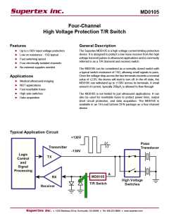
Pin Configurations
Ordering Information
Package Option
NC
B1
18
17
16
15
14
13
12
11
10
1
2
3
4
5
6
7
8
9
NC
A1
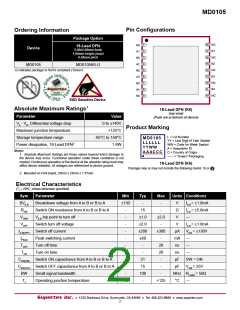
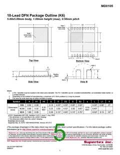
18-Lead DFN
5.00x5.00mm body
1.00mm height (max)
0.50mm pitch
Device
NC
B2
NC
A2
MD0105
MD0105K6-G
NC
B3
-G indicates package is RoHS compliant (‘Green’)
NC
A3
NC
B4
NC
A4
NC
NC
ESD Sensitive Device
Absolute Maximum Ratings1
Parameter
18-Lead DFN (K6)
(top view)
(Pads are at bottom of device)
Value
0 to ±140V
+125°C
VA - VB, Differential voltage drop
Maximum junction temperature
Storage temperature range
Product Marking
L = Lot Number
-65°C to 150°C
1.6W
MD0105
LLLLLL
YY WW
YY = Last Digit of Year Sealed
WW = Code for Week Sealed
A = Assembler ID
Power dissipation, 18-Lead DFN2
Notes:
A AA C CC
C = Country of Origin
1. Absolute Maximum Ratings are those values beyond which damage to
the device may occur. Functional operation under these conditions is not
implied. Continuous operation of the device at the absolute rating level may
affect device reliability. All voltages are referenced to device ground.
= “Green” Packaging
18-Lead DFN (K6)
Package may or may not include the following marks: Si or
2. Mounted on FR4 board, 25mm x 25mm x 1.57mm
Electrical Characteristics
(TJ = 25ºC, unless otherwise specified)
Sym
BVA-B
RSW
Parameter
Min
Typ
-
Max
Units Conditions
Breakdown voltage from A to B or B to A
Switch ON resistance from A to B or B to A
VA-B trip point to turn off
±130
-
V
Ω
IA-B = ±1.0mA
IA-B = ±5.0mA
---
-
15
-
VTRIP
VOFF
-
±1.0
±2.0
±200
±60
-
±2.0
V
Switch turn off voltage
-
-
V
IA-B = ±1.0mA
VA-B = ±130V
IA-B(OFF) Switch off current
-
±300
µA
IPEAK
TOFF
TON
Peak switching current
Turn off time
-
-
mA ---
-
20
ns
ns
pF
pF
---
Turn on time
-
-
20
---
CSW(ON) Switch ON capacitance from A to B or B to A
CSW(OFF) Switch OFF capacitance from A to B or B to A
-
-
21
-
SW = ON
VSW = 25V
15
-
-
BW
TJ
Small signal bandwidth
-
100
-
MHz RLOAD = 50Ω
°C ---
Operating junction temperature
-40
+125
Supertex inc. ● 1235 Bordeaux Drive, Sunnyvale, CA 94089 ● Tel: 408-222-8888 ● www.supertex.com
2

 SUPERTEX [ Supertex, Inc ]