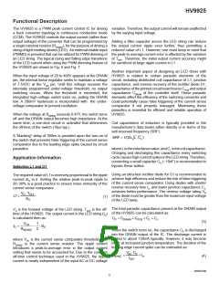
In order to avoid false triggering of the current sense rectified AC line input, the exact equation for calculating the
comparator, CP must be minimized in accordance with the conduction loss is more cumbersome. However, it can be
following expression:
estimated using the following equation:
(10)
PCOND = KC ⋅IO2 ⋅RON + Kd ⋅IDD ⋅ VAC
ISAT ⋅ T
(
− trr
)
BLANK(MIN)
(5)
CP <
V
IN(MAX)
where VAC is the input AC line voltage. The coefficients KC
where TBLANK(MIN) is the minimum blanking time of 200ns, and and Kd can be determined from the minimum duty ratio
VIN(MAX) is the maximum instantaneous input voltage.
Dm=0.71Vo/(ηVAC).
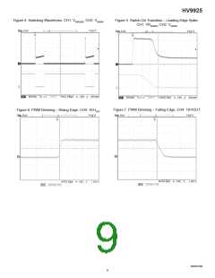
The typical DRAIN and RSENSE voltage waveforms are shown
in Fig. 3 and Fig. 4.
0.7
Estimating Power Loss
0.6
Discharging the parasitic capacitance CP into the DRAIN
output of the HV9925 is responsible for the bulk of the
0.5
switching power loss. It can be estimated using the following
equation:
Kd(Dm)
0.4
Kc(Dm)
2
CPV
IN
(6)
PSWITCH
=
+ VINISAT ⋅ t ⋅F
S
rr
2
0.3
0.2
0.1
where Fs is the switching frequency and ISAT is the saturated
DRAIN current of the HV9925. The switching loss is the
greatest at the maximum input voltage.
The switching frequency is given by the following:
0
0.1
0.2
0.3
0.4
0.5
0.6
0.7
Dm
V
− η−1 ⋅ VO
IN
FS =
(7) Fig. 1. Conduction Loss Coefficients KC and Kd
V ⋅ TOFF
IN
EMI Filter
where η is the efficiency of the power converter.
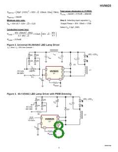
As with all off-line converters, selecting an input filter is critical
When the HV9925 LED driver is powered from the full-wave to obtaining good EMI. A switching side capacitor, albeit of
rectified AC input, the switching power loss can be estimated small value, is necessary in order to ensure low impedance
as:
to the high frequency switching currents of the converter. As
(8) a rule of thumb, this capacitor should be approximately 0.1-
0.2 µF/W of LED output power. A recommended input filter is
shown in Figure 2 for the following design example.
1
PSWITCH
≈
VAC ⋅CP + 2⋅ISAT ⋅ trr
V
− η−1 ⋅ VO
AC
(
)
2⋅ TOFF
VAC is the input AC line voltage.
Design Example 1
The switching power loss associated with turn-off transitions Let us design an HV9925 LED lamp driver meeting the
of the DRAIN output can be disregarded. Due to the large following specifications:
amount of parasitic capacitance connected to this switching
node, the turn-off transition occurs essentially at zero- Input:
Universal AC, 85-264VAC
voltage.
Output Current: 20mA
Load:
String of 10 LED (LW541C by OSRAM
VF = 4.1V max. each)
Conduction power loss in the HV9925 can be calculated as:
PCOND = D⋅IO2 ⋅RON + IDD ⋅ V ⋅ 1− D
(9)
(
)
IN
The schematic diagram of the LED driver is shown in
Fig.2.
where D = VO /ηVIN is the duty ratio, RON is the ON resistance,
IDD is the internal linear regulator current.
When the LED driver is powered from the full-wave
NR021506
6

 SUPERTEX [ Supertex, Inc ]