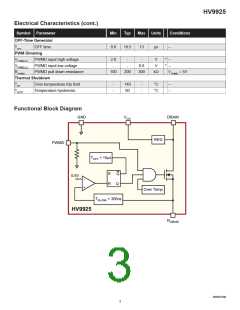
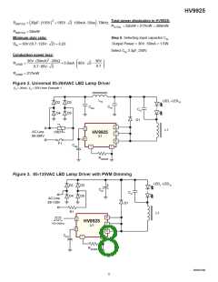
Functional Description
The HV9925 is a PWM peak current control IC for driving variation. Therefore, the output current will remain unaffected
a buck converter topology in continuous conduction mode by the varying input voltage.
(CCM). The HV9925 controls the output current (rather than
output voltage) of the converter that can be programmed by Adding a filter capacitor across the LED string can reduce
a single external resistor (RSENSE), for the purpose of driving a the output current ripple even further, thus permitting a
string of light emitting diodes (LED). An external enable input reduced value of L1. However, one must keep in mind that
(PWMD) is provided that can be utilized for PWM dimming of the peak-to-average current error is affected by the variation
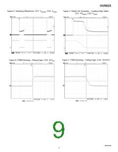
an LED string. The typical rising and falling edge transitions of TOFF. Therefore, the initial output current accuracy might
of the LED current when using the PWM dimming feature of be sacrificed at large ripple current in L1.
the HV9925 are shown in Fig. 6 and Fig. 7.
Another important aspect of designing an LED driver with
When the input voltage of 20 to 400V appears at the DRAIN HV9925 is related to certain parasitic elements of the
pin, the internal linear regulator seeks to maintain a voltage circuit, including distributed coil capacitance of L1, junction
of 7.5VDC at the VDD pin. Until this voltage exceeds the capacitance, and reverse recovery of the rectifier diode D1,
internally programmed under-voltage threshold, no output capacitance of the printed circuit board traces CPCB and output
switching occurs. When the threshold is exceeded, the capacitance CDRAIN of the controller itself. These parasitic
integrated high-voltage switch turns on, pulling the DRAIN elements affect the efficiency of the switching converter and
low. A 200mV hysteresis is incorporated with the under- could potentially cause false triggering of the current sense
voltage comparator to prevent oscillation.
comparator if not properly managed. Minimizing these
parasitics is essential for efficient and reliable operation of
When the voltage at RSENSE exceeds 0.47V, the switch turns HV9925.
off and the DRAIN output becomes high impedance. At the
same time, a one-shot circuit is activated that determines Coil capacitance of inductors is typically provided in the
the off-time of the switch (10µs typ.).
manufacturer’s data books either directly or in terms of the
self-resonant frequency (SRF).
A “blanking” delay of 300ns is provided upon the turn-on of
the switch that prevents false triggering of the current sense
comparator due to the leading edge spike caused by circuit
parasitics.
SRF = 1/(2π L ⋅CL )
whereListheinductancevalue,andCL isthecoilcapacitance.
Charging and discharging this capacitance every switching
cycle causes high-current spikes in the LED string.Therefore,
connecting a small capacitor CO (~10nF) is recommended to
bypass these spikes.
Application Information
Selecting L1 and D1
Using an ultra-fast rectifier diode for D1 is recommended to
achieve high efficiency and reduce the risk of false triggering
of the current sense comparator. Using diodes with shorter
reverse recovery time trr
and lower junction capacitance CJ
achieves better performance. The reverse voltage rating VR
of the diode must be greater than the maximum input voltage
of the LED lamp.
The required value of L1 is inversely proportional to the ripple
current ∆IO in it. Setting the relative peak-to-peak ripple to
20~30% is a good practice to ensure noise immunity of the
current sense comparator.
VO ⋅ TOFF
L1=
(1)
∆IO
The total parasitic capacitance present at the DRAIN output
of the HV9925 can be calculated as:
VO is the forward voltage of the LED string. TOFF is the off-
time of the HV9925. The output current in the LED string (IO)
is calculated then as:
CP = CDRAIN + CPCB + CL + CJ
(3)
VTH
1
2
IO
=
−
⋅ ∆IO
(2)
RSENSE
When the switch turns on, the capacitance CP is discharged
into the DRAIN output of the IC. The discharge current is
limited to about 150mA typically. However, it may become
lower at increased junction temperature. The duration of the
leading edge current spike can be estimated as:
where VTH is the current sense comparator threshold, and
RSENSE is the current sense resistor. The ripple current
introduces a peak-to-average error in the output current
setting that needs to be accounted for. Due to the constant
off-time control technique used in the HV9925, the ripple
current is nearly independent of the input AC or DC voltage
V ⋅CP
ISAT
IN
TSPIKE
=
+ trr
(4)
NR021506
5

 SUPERTEX [ Supertex, Inc ]