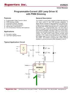
Ordering Information
Package Options
8-Pin SOIC w/ Heat Slug
HV9925SG-G
DEVICE
HV9925
-G indicates package is RoHS compliant (‘Green’)
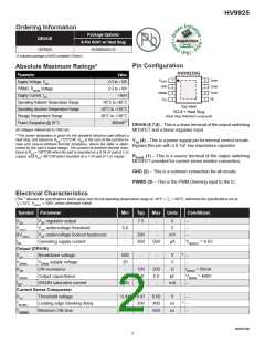
Pin Configuration
Absolute Maximum Ratings*
HV9925SG
Parameter
Value
-0.3 to +10V
-0.3 to +10V
+5mA
Drain
Drain
Drain
NC
RSENSE
GND
1
2
3
4
8
7
6
5
Supply Voltage, VDD
PWMD, RSENSE Voltage
PWMD
VDD
Supply Current, IDD
Operating Ambient Temperature Range
Operating Junction Temperature Range
Storage Temperature Range
Power Dissipation @ 25°C
All voltages referenced to GND pin.
-40°C to +85°C
-40°C to +125°C
-65°C to +150°C
800mW**
top view
SO-8 + Heat Slug
(Heat Slug Potential is at ground)
DRAIN (6,7,8) – This is a drain terminal of the output switching
MOSFET and a linear regulator input.
**The power dissipation is given for the standard minimum pad without a
heat slug, and based on RθJA=125°C/W. RθJA is the sum of the junction-to-
case and case-to-ambient thermal resistance, where the latter is deter-
mined by the user’s board design. The junction-to-ambient thermal resis-
tance is RθJA= 105°C/W when the part is mounted on a 0.04 in2 pad of 1 oz
copper, and RθJA= 60°C/W when mounted on a 1 in2 pad of 1 oz copper.
VDD (4) – This is a power supply pin for internal control circuits.
Bypass this pin with a 0.1uF low impedance capacitor.
RSENSE (1) – This is a source terminal of the output switching
MOSFET provided for current sense resistor connection.
GND (2) – This is a common connection for all circuits.
PWMD (3) – This is the PWM Dimming input to the IC.
Electrical Characteristics
(The *
denotes the specifications which apply over the full operating temperature range of -40°C < TA < +85°C, otherwise the specifications are at
TA = 25°C. VDRAIN = 100V, unless otherwise noted)
Symbol Parameter
VDD VDD regulator output
Min
Typ
Max Units
Conditions
5.0
7.5
V
V
VUVLO
ΔVUVLO
IDD
VDD undervoltage threshold
VDD undervoltage lockout hysteresis
Operating supply current
200
300
mV
μA
500
VDD(EXT) = 8.5V
Output (DRAIN)
Breakdown voltage
500
20
V
VDRAIN
RON
VDRAIN supply voltage
ON resistance
100
1.0
150
200
5.0
Ω
IDRAIN = 50mA
VDRAIN = 400V
CDRAIN
ISAT
Output capacitance
DRAIN saturation current
pF
mA
100
Current Sense Comparator
VTH
Threshold voltage
0.44
200
0.47
300
0.50
400
650
V
TBLANK
TON(MIN)
Leading edge blanking delay
Minimum ON time
ns
ns
NR021506
2

 SUPERTEX [ Supertex, Inc ]