HV7802
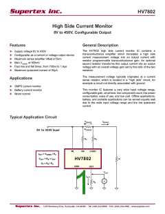
Sense Resistor Considerations
Transient Protection
Limit the sense resistor voltage to 500mV during normal Add a protection resistor (RP) in series with the LOAD pin if
operating conditions. Limit the power dissipation in the sense VSENSE can exceed 5V in positive sense or 600mV in negative
resistor to suit the application; a high sense voltage benefits sense, whether in steady state or in transient conditions.
accuracy, but may result in high power dissipation as well.
A large VSENSE may occur during system startup or shutdown
ConsidertheuseofKelvinconnectionsforapplicationswhere when charging and discharging large capacitors. VSENSE may
considerable voltage drops may occur in the PCB traces. be large due to fault conditions, such as short circuit or a
A layout pattern, which minimizes voltage drops across the broken or missing sense resistor.
sense lines is shown below.
An internal 5V Zener diode with a current rating of 10mA
+ VSENSE
-
protects the sense amplifier inputs. The block diagram
shows the orientation of this diode. The Zener diode provides
clamping at 5V for a positive VSENSE and at 600mV for a
negative VSENSE
.
Limit the Zener current to 10mAunder worst case conditions.
A 100kΩ resistor limits the maximum Zener diode current to
Note that the SpENrSoEtection resistor may affect bandwidth.
The resistor forms a RC network with the trace and pin
capacitance at the LOAD pin. For example, capacitance of
RSENSE
4.5mA when V
is 450V, whether positive or negative.
IN LOAD
Choose a low inductance type sense resistor if preservation 5pF results in a time constant of 500ns.
of bandwidth is important. Kelvin connections help by
minimizing the inductive voltage drops as well. The inductive The protection resistor may cause an offset voltage due to
voltage drop may be substantial when operating at high bias current at the LOAD input. A 100kΩ protection resistor
frequency. A trace or component inductance of just 10nH could cause an offset of 100µV, or 0.2% of full scale, under
contributes an impedance of 6.2mΩ at 100kHz, which worst case bias current. Note that bias current is nominally
constitutes a 6% error when using a 100mΩ sense resistor. zero since LOAD is a high impedance CMOS input, resulting
in zero bias current induced offset voltage.
Pin Description
Pin #
Pin Name
Description
1
IN
Sense amplifier input and supply.
Provides gain setting of the transconductance amplifier. Connect gain setting resistor
(RA) between Pin 1 and Pin 2.
2
3
RA
Sense amplifier input. High impedance input with Zener diode protection. Add an
external protection resistor in series with LOAD if VSENSE exceeds the range of -600mV
to +5V.
LOAD
4
5
NC
NC
No Connect. This pin must be left floating for proper operation
No Connect. This pin must be left floating for proper operation.
Output of the transconductance amplifier. Output current to output voltage conversion
can be accomplished through addition of an external resistor (RB) at this pin. Overall
voltage gain is determined by the ratio of RB to RA.
6
OUT
7
8
NC
No connect. This pin must be left floating for proper operation.
Supply return.
GND
4

 SUPERTEX [ Supertex, Inc ]