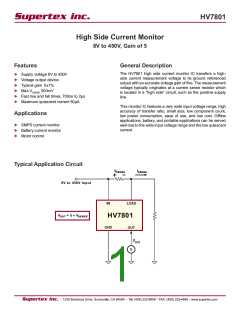
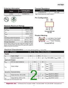
HV7801
Sense Resistor Considerations
Transient Protection
Limit the sense resistor voltage to 500mV during normal Add a protection resistor (R ) in series with the LOAD pin
operating conditions. Limit the power dissipation in the sense if VSENSE can exceed 5V in aPpositive sense or 600mV in a
resistor to suit the application; a high sense voltage benefits negative sense, whether in a steady state or in transient
accuracy, but increases power dissipation.
conditions.
Consider the use of Kelvin connections for applications A large VSENSE may occur during system startup or shutdown
where considerable voltage drops may occur in the PCB due to the charging and discharging of bulk storage
traces. A layout pattern which minimizes voltage across the capacitors. V
may be large due to fault conditions, such
sense lines is shown below.
as a short ciSrEcNuSiEt condition, or a broken or missing sense
resistor.
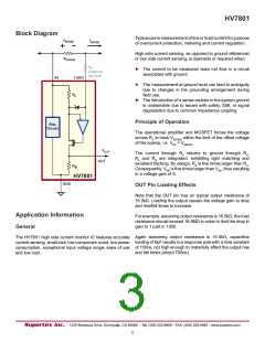
An internal 5V Zener diode with a current rating of ±0mA
protects the sense amplifier inputs. The block diagram
shows the orientation of this diode. The Zener diode provides
clamping at 5V for a positive VSENSE and at 600mV for a
+ VSENSE
-
negative VSENSE
.
Under worst case conditions, limit the Zener current to ±0mA.
A ±00kΩ resistor limits the maximum Zener diode current to
4.5mA when VSENSE is 450V, whether positive or negative.
Note that the protection resistor may affect the bandwidth.
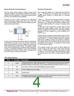
RSENSE
IN LOAD
Choose a low inductance type sense resistor if preservation The resistor forms an RC network with the trace and pin
of bandwidth is important. The use of Kelvin connections capacitance at the LOAD pin. A capacitance of 5pF results
helps by excluding the inductive voltage drop across the in a time constant of 500ns.
traces leading to the sense resistor. The inductive voltage
drop may be substantial when operating at high frequencies. The protection resistor may cause an offset voltage due
A trace or component inductance of just ±0nH contributes to bias current at the LOAD input. Under worst case bias
an impedance of 6.2mΩ at ±00kHz, which constitutes a 61 current, a ±00kΩ protection resistor could cause an offset
error when using a ±00mΩ sense resistor.
of ±00µV or 0.21 of full scale. Note that the bias current
is nominally zero as the LOAD is a high impedance CMOS
input.
Pin Description
Pin #
Pin Name
Description
Sense amplifier input. High impedance input with Zener diode protection. Add an external
protection resistor in series with LOAD if VSENSE exceeds the range of -600mV to +5V.
±
LOAD
2
3
4
NC
IN
No connect. This pin must be left floating for proper operation.
Sense amplifier input and supply.
Supply return.
GND
Output with a nominal output resistance of ±6.5kΩ. Preservation of accuracy may require
an external buffer amplifier to prevent excessive loading.
5
OUT
4

 SUPERTEX [ Supertex, Inc ]