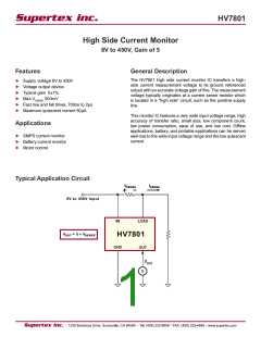
HV7801
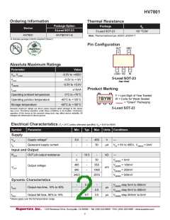
Ordering Information
Thermal Resistance
Package Option
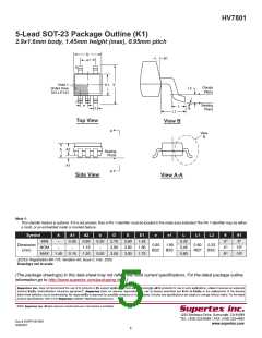
5-Lead SOT-23
HV780±K±-G
Package
θja
±9± OC/W
Device
5-Lead SOT-23
Note: Thermal testboard per JEDEC JESD51-7
HV780±
-G indicates package is RoHS compliant (‘Green’)
Pin Configuration
OUT
5
GND
4
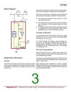
Absolute Maximum Ratings
2
3
±
Parameter
Value
-0.5V to +450V
-0.5V to +±0V
-0.5V to +5.0V
±±0mA
LOAD NC
IN
VIN, VLOAD
5-Lead SOT-23
VOUT
(top view)
VSENSE
Product Marking
ILOAD
Operating ambient temperature
Operating junction temperature
Storage temperature
Absolute maximum ratings are those values beyond which damage to the device
may occur. Functional operation under these conditions is not implied. Continuous
operation of the device at the absolute rating level may affect device reliability. All
voltages are referenced to device ground.
0°C to +70°C
-40°C to +±25°C
-65°C to +±50°C
Y = Last Digit of Year Sealed
W = Code for Week Sealed
= “Green” Packaging
7BYW
5-Lead SOT-23
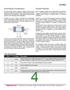
Electrical Characteristics (TA = 25°C unless otherwise specified, VIN = 8.0V to 450V)
Symbol
Parameter
Min
Typ
Max Units Conditions
Supply
VIN
Supply voltage*
8.0
-
-
-
450
50
V
---
IQ
Quiescent supply current
µA
VIN = 8V to 450V, VSENSE = 0mV
Input and Output
ROUT
OUT pin output resistance
-
±6.5
-
kΩ
---
0
-
-
-
-
50
VSENSE = 0mV
VSENSE = ±00mV
VSENSE = 200mV
VSENSE = 500mV
445
940
2425
555
±060
2575
Output voltage
VOUT
mV
Dynamic Characteristics
-
-
-
0.7
-
-
VSENSE step 5mV to 500mV
VSENSE step 0mV to 500mV
VSENSE step 500mV to 0mV
tRISE
Output rise time, ±01 to 901
µs
µs
2.0
2.0
tFALL
Output fall time, 901 to ±01
0.7
*Values apply over the full temperature range.
2

 SUPERTEX [ Supertex, Inc ]