HV5522/HV5530/HV5622/HV5630
Electrical Characteristics (over recommended operating conditions unless noted)
DC Characteristics
Symbol
Parameter
Min
Max
Units Conditions
IDD
VDD supply current
15
mA
fCLK = 8MHz
FDATA = 4MHz
IDDQ
Quiescent VDD supply current
Off state output current
100
10
µA
µA
VIN = 0V
IO(OFF)
All outputs high
All SWS parallel
IIH
High-level logic input current
Low-level logic input current
High-level output data out
1
µA
µA
V
VIH = VDD
IIL
-1
VIL = 0V
VOH
VDD - 1.0V
IDout = -100µA
IHVout = +100mA
IDout = +100µA
IOL = -100mA
HVOUT
15.0
1.0
V
VOL
Low-level output voltage
HVOUT clamp voltage
Data out
V
VOC
-1.5
V
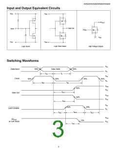
AC Characteristics (VDD = 12V, TC = 25°C)
Symbol
fCLK
tW
Parameter
Min
Max
Units Conditions
Clock frequency
8
MHz
ns
Clock width high or low
62
25
10
tSU
Data set-up time before clock falls
Data hold time after clock falls
Turn on time, HVOUT from enable
Delay time clock to data high to low
Delay time clock to data low to high
Delay time clock to LE low to high
Width of LE pulse
ns
tH
ns
tON
500
100
100
ns
ns
ns
ns
ns
ns
RL = 2KΩ to VPP MAX
tDHL
tDLH
tDLE
tWLE
tSLE
CL = 15pF
CL = 15pF
50
50
50
LE set-up time before clock falls
Recommended Operating Conditions
Symbol
Parameter
Min
Max
13.2
+300
+220
VDD
2.0
Units
V
VDD
Logic supply voltage
High voltage output
10.8
-0.3
HV5530 and HV5630
HV5522 and HV5622
V
HVOUT
-0.3
V
VIH
VIL
fCLK
TA
High-level input voltage
Low-level input voltage
Clock frequency
VDD - 2V
0
V
V
8
MHz
°C
°C
Operating free-air temperature
Plastic
-40
-55
+85
+125
Ceramic
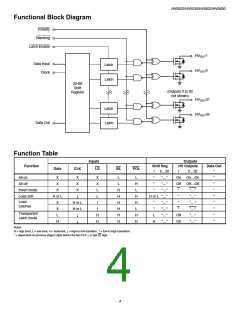
Note:
Power-up sequence should be the following:
1. Connect ground.
2. Apply VDD
.
3. Set all inputs to a known state.
Power-down sequence should be the reverse of the above.
2

 SUPERTEX [ Supertex, Inc ]