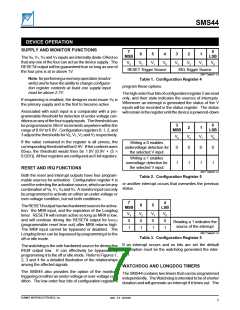
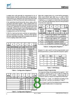
SMS44
I nput Data Protocol
One data bit is transferred during each clock pulse. The
data on the SDA line must remain stable during clock high
time, because changes on the data line while SCL is high
will be interpreted as start or stop condition.
The protocol defines any device that sends data onto the
busasa“transmitter”andanydevicethatreceivesdataas
a “receiver.” The device controlling data transmission is
called the “master” and the controlled device is called the
“slave.” In all cases the SMS44 will be a “slave” device,
since it never initiates any data transfers.
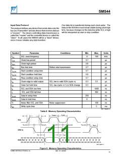
Sym bol
fSCL
Param eter
SCL clock frequency
Clock low period
Conditions
Min.
0
Ma.x
U nist
kHz
µs
µs
µs
µs
µs
µs
µs
µs
ns
ns
ns
ns
ns
100
tLOW
tHIGH
tBUF
4.7
4.0
4.7
4.7
4.0
4.7
0.3
0.3
Clock high period
Bus free time
Before new transmission
tSU:STA
tHD:STA
tSU:STO
tAA
Start condition setup time
Start condition hold time
Stop condition setup time
Clock edge to valid output
Data Out hold time
SCL and SDA rise time
SCL and SDA fall time
Data In setup time
SCL low to valid SDA (cycle n)
3.5
tDH
SCL low (cycle n+1) to SDA change
tR
1000
300
tF
tSU:DAT
tHD:DAT
TI
250
0
Data In hold time
Noise filter SCL and SDA
Write cycle time
Noise suppression
100
5
tWR
ms
2047 Table08 2.2
Table 8 .
Memory Operati ng Characteri sti cs
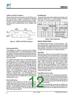
t
t
LOW
HIGH
t
t
R
F
SCL
t
t
t
t
SU:STO
t
HD:DAT
SU:STA
SU:DAT
HD:STA
t
BUF
SDA I n
SDA Out
t
t
AA
DH
2047 Fig08 2.1
Fi gure 8 .
Memory Operati ng Characteri sti cs
SUMMIT MICROELECTRONICS, Inc.
2047 2.3 10/23/00
11

 SUMMIT [ SUMMIT MICROELECTRONICS, INC. ]