SMM465
Preliminary Information
I2C PROGRAMMING INFORMATION (CONTINUED)
WRITE PROTECTION
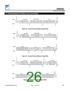
The word address must be set each time the memory
is accessed. Memory writes and reads are shown in
Figures 22, 23 and 24.
The SMM465 powers up into a write protected mode.
Writing a code to the volatile write protection register
can disable the write protection. The write protection
register is located at address 87HEX of slave address
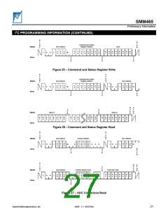
COMMAND AND STATUS REGISTERS
The command and status registers are located at
1001BIN
.
slave address 1001BIN
.
Writes and reads of the
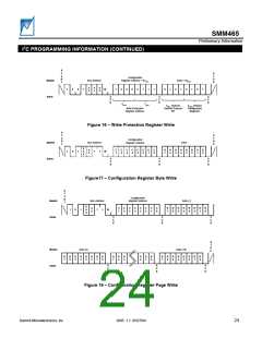
Writing 0101BIN to bits [7:4] of the write protection
register allow writes to the general-purpose memory
while writing 0101BIN to bits [3:0] allow writes to the
configuration registers. The write protection can re-
enable by writing other codes (not 0101BIN) to the write
protection register. Writing to the write protection
register is shown in Figure 16.
command and status registers are shown in Figures
25 and 26.
ADC CONVERSIONS
An ADC conversion on any monitored channel can be
performed and read over the I2C bus using the ADC
read command. The ADC read command, shown in
Figure 27, starts with a dummy write to the 1001BIN
slave address. Bits [6:3] of the word address byte are
used to address the desired monitored input. Once
the device acknowledges the channel address, it
begins the ADC conversion of the addressed input.
This conversion requires 70µs to complete. During
this conversion time, acknowledge polling can be
used. The SMM465 will not acknowledge the address
bytes until the conversion is complete. When the
conversion has completed, the SMM465 will
acknowledge the address byte and return the 10-bit
conversion along with a 4-bit channel address echo.
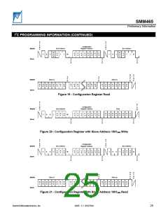
CONFIGURATION REGISTERS
The majority of the configuration registers are grouped
with the general-purpose memory located at either
slave address 1010BIN or 1011BIN. The bus address
bits, A[1:0], used to differentiate the general-purpose
memory from the configuration registers are set to
11BIN. Bus address bit A[2] can be programmed as
either 0 or biased by the A2 pin.
Two additional configuration registers are located at
addresses 83HEX and 84HEX of slave address 1001BIN
.
Writing and reading the configuration registers is
GRAPHICAL USER INTERFACE (GUI)
shown in Figures 17, 18, 19, 20 and 21
Device configuration utilizing the Windows based
SMM465 graphical user interface (GUI) is highly
recommended. The software is available from the
Summit website (www.summitmicro.com). Using the
GUI in conjunction with this datasheet and Application
Note 33, simplifies the process of device prototyping
and the interaction of the various functional blocks. A
programming Dongle (SMX3200) is available from
Summit to communicate with the SMM465. The
Dongle connects directly to the parallel port of a PC
and programs the device through a cable using the I2C
bus protocol.
Note: Configuration writes or reads of registers 00HEX
to 0FHEX should not be performed while the SMM465 is
margining.
GENERAL-PURPOSE MEMORY
The 4k-bit general-purpose memory is located at
either slave address 1010BIN or 1011BIN
.
The bus
address bits, A[1:0], used to differentiate the general-
purpose memory from the configuration registers are
set to 00BIN for the first 2k-bits and 01BIN for the second
2k-bits. Bus address bit A[2] can be programmed as
either 0 or biased by the A2 pin.
Slave Address Bus Address Register Type
Write Protection Register,
Command and Status Registers,
Two Configuration Registers,
ADC Conversion Readout
1001BIN
A2 A1 A0
A2 0 0
A2 0 1
A2 1 1
1st 2-k Bits of General-Purpose Memory
2nd 2-k Bits of General-Purpose Memory
Configuration Registers
1010BIN
or
1011BIN
Table 1 - Address bytes used by the SMM465.
Summit Microelectronics, Inc
2085 1.1 05/27/04
23

 SUMMIT [ SUMMIT MICROELECTRONICS, INC. ]