VN5770AK-E
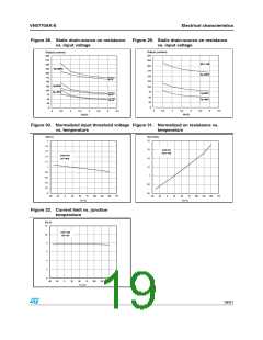
Electrical characteristics
3.2
Electrical characteristics for low side switches
Note:
Values specified in this section are for -40°C < Tj < 150°C, unless otherwise specified
Table 12. Off
Symbol
Parameter
Test Conditions
VIN=0V; ID=1.5A
VIN=0V; ID=2mA
DS=VIN; ID=1mA
Min
Typ
Max
Unit
Drain-source Clamp
Voltage
VCLAMP
40
45
55
V
Drain-source Clamp
Threshold Voltage
VCLTH
VINTH
IISS
36
V
V
Input Threshold
Voltage
V
0.5
2.5
Supply Current from
Input Pin
VDS=0V; VIN=5V
100
6.8
150
µA
V
IIN=1mA
IIN=-1mA
6
8
Input-Source Clamp
Voltage
VINCL
-1.0
-0.3
Zero Input Voltage
Drain Current
(VIN=0V)
VDS=13V; VIN=0V; Tj=25°C
30
75
IDSS
µA
VDS=25V; VIN=0V
Table 13. On
Symbol
Parameter
Test Conditions
Min
Min
Typ
Typ
Max
Unit
VIN=5V; ID=3A; Tj=25°C
VIN=5V; ID=3A
120
240
Static Drain-source
On Resistance
RDS(on)
mΩ
Table 14. Dynamic (Tj=25°C, unless otherwise specified)
Symbol
Parameter
Test Conditions
VDD=13V; ID=1.5A
VDS=13V; f=1MHz; VIN=0V
Max Unit
Forward
gfs
2.5
S
Transconductance
Output Capacitance
COSS
150
pF
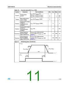
Table 15. Switching (Tj=25°C, unless otherwise specified)
Symbol
Parameter
Test Conditions
Min
Typ
Max Unit
td(on)
tr
td(off)
tf
td(on)
tr
td(off)
tf
Turn-on Delay Time
Rise Time
200
1.2
400
2.5
ns
µs
ns
ns
µs
µs
µs
µs
VDD=15V; ID=3A
Vgen=5V; Rgen=RIN MINn=220Ω
Turn-off Delay Time
Fall Time
600 1350
400 1000
Turn-on Delay Time
Rise Time
0.80
3.7
2.5
7.5
7.5
7.0
VDD=15V; ID=3A
Vgen=5V; Rgen=2.2KΩ
Turn-off Delay Time
Fall Time
2.6
2.3
15/31

 STMICROELECTRONICS [ ST ]