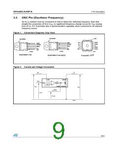
VIPer50A-E/ASP-E
5 Operation Description
V
is the voltage hysteresis of the UVLO logic (refer to the minimum specified value).
DDhyst
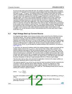
The soft start feature can be implemented on the COMP pin through a simple capacitor which
will be also used as the compensation network. In this case, the regulation loop bandwidth is
rather low, because of the large value of this capacitor. In case a large regulation loop
bandwidth is mandatory, the schematics of (see Figure 17) can be used. It mixes a high
performance compensation network together with a separate high value soft start capacitor.
Both soft start time and regulation loop bandwidth can be adjusted separately.
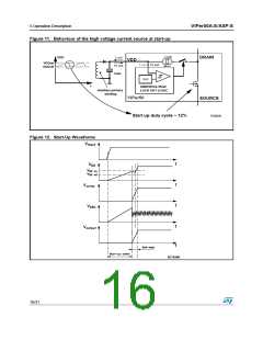
If the device is intentionally shut down by tying the COMP pin to ground, the device is also
performing start-up cycles, and the V voltage is oscillating between V
and V
.
DD
DDon
DDoff
This voltage can be used for supplying external functions, provided that their consumption does
not exceed 0.5mA. (see Figure 18) shows a typical application of this function, with a latched
shutdown. Once the "Shutdown" signal has been activated, the device remains in the Off state
until the input voltage is removed.
5.4
Transconductance Error Amplifier
The VIPer50A-E/ASP-E includes a transconductance error amplifier. Transconductance Gm is
the change in output current (I
) versus change in input voltage (V ). Thus:
COMP
DD
∂lCOMP
Gm = ------------------
∂VDD
The output impedance Z
at the output of this amplifier (COMP pin) can be defined as:
COMP
V
∂
1
Gm
∂VCOMP
∂VDD
COMP
ZCOMP = --------------------= ------- × ------------------------
I
∂
COMP
This last equation shows that the open loop gain A
can be related to G and Z :
COMP
VOL
m
A
= G x Z
m COMP
VOL
where G value for VIPer50A-E/ASP-E is 1.5 mA/V typically.
m
G is defined by specification, but Z
and therefore A
are subject to large tolerances.
m
COMP
VOL
An impedance Z can be connected between the COMP pin and ground in order to define the
transfer function F of the error amplifier more accurately, according to the following equation
(very similar to the one above):
F
= Gm x Z(S)
(S)
The error amplifier frequency response is reported in Figure 10. for different values of a simple
resistance connected on the COMP pin. The unloaded transconductance error amplifier shows
an internal Z
of about 330KΩ. More complex impedance can be connected on the COMP
COMP
pin to achieve different compensation level. A capacitor will provide an integrator function, thus
eliminating the DC static error, and a resistance in series leads to a flat gain at higher
frequency, insuring a correct phase margin. This configuration is illustrated in Figure 20
As shown in Figure 19 an additional noise filtering capacitor of 2.2nF is generally needed to
avoid any high frequency interference.
Is also possible to implement a slope compensation when working in continuous mode with
duty cycle higher than 50%. Figure 21 shows such a configuration. Note: R1 and C2 build the
classical compensation network, and Q1 is injecting the slope compensation with the correct
polarity from the oscillator sawtooth.
13/31

 STMICROELECTRONICS [ ST ]